Part 14: Combinational Logic in Verilog: Explained with 5 Examples
2025-05-05 | By DWARAKAN RAMANATHAN
Introduction:
Combinational logic is one of the fundamental concepts in digital circuit design, where the output depends solely on the current inputs, with no memory of previous states. Verilog, a hardware description language (HDL), is widely used for designing digital systems. I will explain combinational logic in Verilog, followed by 5 detailed examples, including RTL (Register Transfer Level) code and test benches.
In combinational logic circuits, the output is determined by the present state of the inputs. The key feature of combinational circuits is that they have no memory, meaning their outputs change instantly when inputs change. Examples include adders, multiplexers, and logic gates (AND, OR, NOT).
Verilog enables the modeling of these circuits by defining logic expressions, which are executed whenever the inputs change.
Key Characteristics of Combinational Logic:
- No Memory: The circuit has no state element that stores past information.
- Instantaneous Output: The output changes immediately as inputs change.
- Purely Deterministic: Given a set of inputs, the output is always predictable.
Verilog Constructs for Combinational Logic
Verilog allows us to implement combinational logic using the assign statement for continuous assignments or always blocks with @* for implicit sensitivity lists. Below are the 5 examples that demonstrate different aspects of combinational logic in Verilog.
Example 1: AND Gate
Verilog Code:
module and_gate(input a, input b, output c); assign c = a & b; // Continuous assignment for AND gate endmodule
Testbench:
module tb_and_gate;
reg a, b;
wire c;
// Instantiate the and_gate module
and_gate uut(a, b, c);
initial begin
// Test different combinations of inputs
$monitor("a = %b, b = %b, c = %b", a, b, c);
// Apply test cases
a = 0; b = 0; #10;
a = 0; b = 1; #10;
a = 1; b = 0; #10;
a = 1; b = 1; #10;
$finish;
end
endmodule
Explanation:
An AND gate is a fundamental logic gate that performs a logical multiplication operation. It produces a high output (1) only when all of its inputs are high (1). If any input is low (0), the output remains low (0). This behavior makes the AND gate useful in circuits where multiple conditions must be satisfied simultaneously. Mathematically, the AND operation can be expressed as 𝑌=𝐴⋅𝐵.
Y=A⋅B, where A and B are the inputs, and Y is the output. The AND gate is widely used in control logic, authentication systems, and digital decision-making circuits. For example, in an authentication system, access is granted only when both a username and password are correct, which aligns with the AND gate's logic. It is also commonly found in multipliers, data validation systems, and digital security circuits where multiple inputs must be true for an action to occur.
Testbench. The testbench sets different values of a and b and monitors the output c.
Example 2: OR Gate
Verilog Code:
module or_gate(input a, input b, output c); assign c = a | b; // Continuous assignment for OR gate endmodule
Testbench:
module tb_or_gate;
reg a, b;
wire c;
or_gate uut(a, b, c);
initial begin
$monitor("a = %b, b = %b, c = %b", a, b, c);
a = 0; b = 0; #10;
a = 0; b = 1; #10;
a = 1; b = 0; #10;
a = 1; b = 1; #10;
$finish;
end
endmodule
Explanation:
An OR gate is another fundamental logic gate that performs a logical addition operation. It produces a high output (1) if at least one of its inputs is high (1). The output remains low (0) only when all inputs are low (0). This makes OR gates essential in systems where the occurrence of any one event should trigger an action. Mathematically, an OR gate follows the equation 𝑌=𝐴+𝐵.
Y=A+B, where A and B are the inputs, and Y is the output. OR gates are widely used in alarm systems, signal detection, and logic circuits where at least one condition needs to be met. For instance, in a fire alarm system, the alarm should activate if either smoke is detected, or the temperature exceeds a critical threshold. Similarly, OR gates play a crucial role in microprocessor flag registers, multiplexers, and digital communication systems, where signals from multiple sources need to be combined for decision-making or data transmission.
Testbench: This tests all input combinations, revealing the truth table of the OR gate.
Example 3: 4-bit Adder (Sum of Two 4-bit Numbers)
Verilog Code:
module adder_4bit(input [3:0] a, input [3:0] b, output [3:0] sum, output carry_out);
assign {carry_out, sum} = a + b; // Continuous assignment for addition
endmodule
Testbench:
module tb_adder_4bit;
reg [3:0] a, b;
wire [3:0] sum;
wire carry_out;
adder_4bit uut(a, b, sum, carry_out);
initial begin
$monitor("a = %b, b = %b, sum = %b, carry_out = %b", a, b, sum, carry_out);
a = 4'b0011; b = 4'b0101; #10;
a = 4'b1111; b = 4'b0001; #10;
a = 4'b1000; b = 4'b1000; #10;
a = 4'b0000; b = 4'b0000; #10;
$finish;
end
endmodule
Explanation:
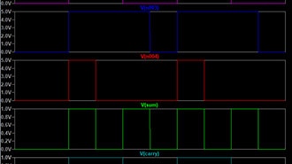
A binary adder is a combinational circuit that performs binary addition. A 4-bit binary adder consists of four full adders in cascade, each adding corresponding bits of two 4-bit binary numbers and a carry from the preceding bit position. The addition follows the rules of binary arithmetic: 0 + 0 = 0, 0 + 1 = 1, 1 + 0 = 1, and 1 + 1 = 10 (with a sum of 0 and a carry of 1). The LSB adder has an external carry-in (Cin), whereas the MSB can generate a carry-out (Cout). Binary adders are elementary building blocks in ALUs, counters, and arithmetic circuits and are of elementary importance in computational logic and processor design. Testbench: This tests the adder with different 4-bit inputs and monitors the sum and carry-out.
Example 4: Multiplexer (2-to-1 Mux)
Verilog Code:
module mux_2to1(input a, input b, input sel, output y); assign y = (sel) ? b : a; // Multiplexer logic endmodule
Testbench:
module tb_mux_2to1;
reg a, b, sel;
wire y;
mux_2to1 uut(a, b, sel, y);
initial begin
$monitor("a = %b, b = %b, sel = %b, y = %b", a, b, sel, y);
a = 0; b = 1; sel = 0; #10;
a = 0; b = 1; sel = 1; #10;
a = 1; b = 0; sel = 0; #10;
a = 1; b = 0; sel = 1; #10;
$finish;
end
endmodule
Explanation:
A multiplexer (MUX) is a combinational circuit that chooses one of many input signals and directs the selected input to a shared output. The choosing is by a group of control signals referred to as the select lines. In a 4-to-1 multiplexer, there are four input signals (I0, I1, I2, I3) and a single output signal (Y) and choosing is by two select lines (S0, S1). The multiplexer's operation is simple: when the select lines have different binary values, they decide which of the four input lines is directed to the output. For example, if S1S0 = 00, then Y = I0; if S1S0 = 01, then Y = I1; if S1S0 = 10, then Y = I2; and if S1S0 = 11, then Y = I3. Multiplexers are a digital circuit building block because they have universal applications for data selection and signal routing. Multiplexers are used widely for the efficient selection of data sources in arithmetic logic units (ALUs), communication systems, and other digital systems.
Testbench: It simulates all combinations of the inputs a, b, and sel to illustrate the behavior of the mux.
Example 5: 4-bit Comparator
Verilog Code:
module comparator_4bit(input [3:0] a, input [3:0] b, output eq, output lt, output gt); assign eq = (a == b); // Equality check assign lt = (a < b); // Less than check assign gt = (a > b); // Greater than check endmodule
Testbench:
module tb_comparator_4bit;
reg [3:0] a, b;
wire eq, lt, gt;
comparator_4bit uut(a, b, eq, lt, gt);
initial begin
$monitor("a = %b, b = %b, eq = %b, lt = %b, gt = %b", a, b, eq, lt, gt);
a = 4'b0101; b = 4'b0101; #10;
a = 4'b0011; b = 4'b1001; #10;
a = 4'b1100; b = 4'b0100; #10;
$finish;
end
endmodule
Explanation:
A 4-bit comparator is a combinational circuit that determines the relationship between two 4-bit binary numbers. It takes two 4-bit inputs, usually A and B, and provides three outputs: A is larger than B (A > B), A is equal to B (A = B), and A is smaller than B (A < B). It compares bit by bit from the most significant bit (MSB) to the least significant bit (LSB). Whenever the two numbers' MSB is not the same, the comparator instantly determines that one number is larger. When the two numbers' MSBs are the same, it proceeds to the next significant bit until the difference or until the bits are equal.
Testbench: The testbench covers all the conditions between two 4-bit numbers.
Note: You can always go to the Intel Quartus Prime Tutorial and MODELSIM Tutorials to get the simulations and verify your design. Click here for the Intel Quartus Prime tutorial and here for the MODELSIM tutorial.
Conclusion
Combinational logic in Verilog is powerful for the design and simulation of numerous logic functions. The examples above are simple in terms of logic gates, arithmetic logic functions, multiplexers, and comparators. It can be indicated that Verilog can effectively be used to describe and implement the functions. A crucial role in verifying that the output acts as expected for all possible input combinations comes through testbenches.