Balancing Power Consumption and Performance in Wireless Sensor Designs
投稿人:电子产品
2013-04-11
Whether powered by batteries or even energy scavenging, wireless sensor designs require careful balancing of power requirements and operational capability to meet performance goals. For engineers, that translates into careful selection of MCUs and transceivers capable of meeting tight power budgets while delivering sensor data over wireless networks that can vary in range and sensitivity. This article will demonstrate how these design objectives can be met using a broad array of MCUs, transceivers, and integrated solutions from suppliers such as ams, EnOcean, Maxim Integrated, Microchip Technology, Silicon Labs, and Texas Instruments.
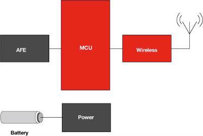
In its most basic form, a wireless sensor comprises a host MCU and wireless transceiver, as well as power subsystem and an analog front end (AFE) of varying complexity depending on the application (Figure 1). For designers, ensuring both extended range and maximum power efficiency of wireless sensor designs requires careful selection of ultra-low-power MCUs and radios.

Although active power consumption specifications quoted in datasheets may be sufficient in some cases, selection typically requires a broader look at device performance characteristics associated with the device's available low-power operating modes. For example, an MCU that specs out with slightly higher active power requirements than another might still provide superior overall power savings if it offers different options for low-power modes and if it includes features and characteristics that ensure maximum time spent in its lowest power modes.
That notion of heightened efficiency fuels a trend toward use of 16- and even 32-bit MCUs in applications long considered the sole domain of 8-bit MCUs. With their wider data paths, 16- and 32-bit MCUs offer greater code density that in many cases allows for more efficient code execution – translating to faster completion of tasks and a quicker return to low-power sleep modes.
Perhaps even more important for power-sensitive applications, advanced MCUs combine ultra-low-power operating modes with fast wake-up times. In the constant cycling between sleep and active mode, a more prolonged wake-up process adds up to a greater proportion of power wasted on an unproductive MCU state.
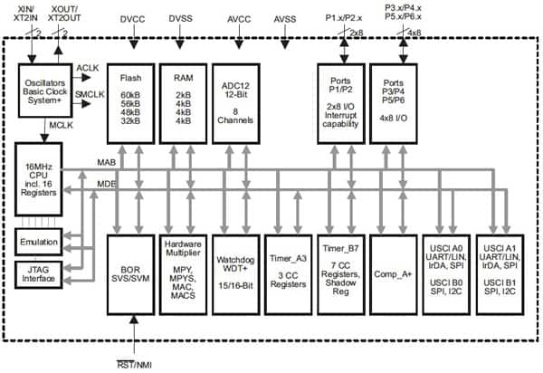
MCUs intended for low-power applications typically feature wake-up times of 1 µs or less. Just as important, these MCUs integrate all the key peripherals required for those target applications. For example, the Texas Instruments MSP430F23x/24x/2410 series (Figure 2) comprises a wide range of devices supplied with different memory configurations and tuned to support specific classes of applications through inclusion of different combinations of peripherals. The TI MSP430F249 includes 60Kbytes+256 bytes of Flash memory and 2 Kbytes of RAM on-chip – and like other members of the series, offers peripherals essential for sensor applications.

To support the needs of data acquisition in sensor applications, MCUs in the family include a high-speed 12-bit ADC with internal reference, sample-and-hold, and autoscan. In addition, family devices include two built-in 16-bit timers, a comparator, four (two in MSP430F23x) universal serial communication interface (USCI) modules, and up to 48 I/O pins. (The MSP430F24x1 devices lack the 12-bit ADC but are otherwise identical to the MSP430F24x devices.)
At the heart of the architecture, a 16-bit RISC CPU works with 16-bit registers and special features such as constant generators to help maximize code efficiency. With its RISC architecture and 62.5 ns instruction cycle time, the MSP430 family can work efficiently through code sets to quickly complete software tasks in active mode – and so return rapidly to its power-conserving low-power modes. To help speed transition back to active mode, the devices include a calibrated digitally controlled oscillator that enables MSP430 MCUs to wake up from low-power modes to active mode in less than 1 µs.
To address low-power requirements in applications such as wireless sensor designs, the MSP430 MCUs offer five different low-power operating modes and operate at low supply voltages, ranging from 1.8 to 3.6 V. In active mode, power consumption is 270 µA (1 MHz, 2.2 V) and falls to 0.3 µA in standby mode and down to 0.1 µA in its off mode with RAM retention.
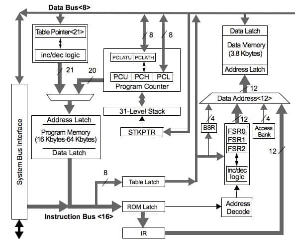
With its line of PIC MCUs, Microchip offers additional options for ultra-low-power operations with devices that feature five power modes and blend 8- and 16-bit architectures (Figure 3). The Microchip PIC18F46J50 MCU offers 64 KB flash and 3.7 KB RAM while operating at 280 µA/MHz in active mode. The PIC18F46J50 power consumption falls to 2.3 mA in idle mode (CPU off, peripherals on) and drops to 105 nA in sleep mode (CPU off, peripherals off, SRAM on). From idle mode, wake-up time is 300 ns, and wake-up time from sleep modes varies from 250 ns for the lightest sleep mode and 300 µs for the deepest mode.

Available 32-bit MCUs continue to show improved low-power performance. For example, the Silicon Labs ARM® Cortex™-M3-based SiM3L1xx MCUs feature power consumption at 175 µA/MHz in active mode, where the processor is executing from flash memory and only 140 µA/MHz when executing from SRAM. In sleep mode with the real-time clock enabled, power consumption is only 250 nA.
These MCUs feature seven power modes and provide additional power-saving features such as disabling clocks for inactive peripherals. Conversely, the processor itself can be placed in a sleep state while peripherals continue to operate, waking the processor when required. The processor can return to active mode from this low-power mode in only four or five clock cycles.
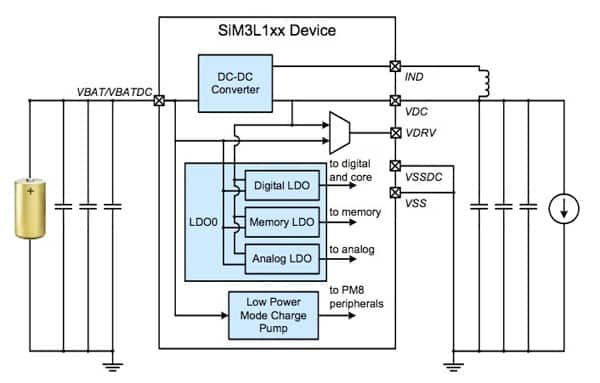
A key contributor to the device's low power is an integrated DC/DC buck converter (Figure 4), able to reduce active-mode power by 40 percent compared to earlier 32-bit MCUs. SiM3L1xx devices also include three low dropout regulators – one to power the analog subsystems, another to power the flash and SRAM memory at 1.8 V, and one to power the digital and core circuitry. Each LDO can be independently powered from the DC/DC converter or directly from the battery voltage. Furthermore, their outputs are adjustable to conserve system power. SiM3L1xx devices also include a low power charge pump for use in low power modes to further reduce power consumption.

Low-power transceivers
With the growing availability of power-efficient MCUs, the concern becomes one of ensuring wireless performance at minimal power while meeting the maximum range requirements of the application. Although customer requirements may dictate the appropriate operating frequency, engineers nevertheless can find themselves faced with a difficult choice influenced by factors including path loss issues and environmental effects.
For typical industrial wireless sensor applications, path loss concerns can drive frequency selection. Lower frequency signals operate with less attenuation across a wide area and range of operating conditions. This observation is evident in the Friis transmission equation:

Where:
Pr = received power
Pt = transmitted power
Gr = receiver gain
Gt = transmitter gain
λ = wavelength
r = distance between receiver and transmitter antennas
Longer wavelength means greater range. Greater range not only translates to less power required for a given radio link budget, but also means that fewer wireless receivers are needed to support a given area – resulting in lower overall-systems cost.
In a study comparing path loss at different frequencies, the Communications Research Centre Canada empirically demonstrated the basic results of the Friis equation, but also showed how environmental factors can profoundly affect range. In their study, researchers measured power at locations with widely differing characteristics and found that the path loss at 2,500 MHz is 11 to 15 dB greater than that at 700 MHz (Figure 5).
| Site No. | Environment Type | Mean (dB) | Standard Deviation (dB) |
| 1 | Open Rural | 10.8 | 6.1 |
| 2 | Forested Rural | 11.3 | 5.0 |
| 3 | Hilly Forested Rural | 18.4 | 5.8 |
| 4 | Suburban | 11.9 | 5.6 |
| 5 | Urban | 14.3 | 5.6 |
Figure 5: In a study, path loss at 2,500 MHz was 11 to 15 dB greater than that at 700 MHz, with the greatest disparity in areas of greater obstruction. (Courtesy of the Communications Research Centre Canada.)
Furthermore, issues beyond path loss can arise in some applications. For example, as wireless sensor applications move physically closer to the human body for health and medical wireless sensor applications, safety issues impact selection of frequency. For example, limitations on recommended exposure rates for higher-frequency radio signals may dictate use of lower-frequency devices such as the ams AS3900, which operates at 27 MHz. For applications requiring wireless communications close to the human body, use of low operating frequencies is desirable due to the low specific absorption rates by tissue at lower frequency.
Intended for relatively low-bitrate applications, the AS3900 is a low-power FSK transceiver that can be configured as transceiver, transmitter-only, or receiver-only system to function at an operating frequency determined by the frequency of an external oscillator. The device works with a supply voltage between 2.0 V to 3.6 V and consumes only 3.8 mA Rx, 4.9 mA @ 0 dBm Tx or 7.6 mA at its maximum output power of 10 dBm. In polling mode, average current consumption is only 2.5 μA and power-down mode consumes only 700 nA.
The AS3900 includes a real-time-clock, wake-up feature, and link manager that enable autonomous control of communication events - reducing or even eliminating the need for an external MCU in some applications. The AS3900 includes a serial digital interface and supports data transfer in burst mode (bi-directional, controlled by link manager), semi-continuous (bi-directional, controlled by microcontroller) and continuous mode (unidirectional, controlled by microcontroller) and requires only a small number of external components.
For operation in more typical sub-GHz ISM bands, engineers can choose from a broad array of transceivers such as the Microchip MRF89XA and TI CC1101 among many others. These devices typically offer operation in a number of distinct ISM bands and offer specialized features designed to minimize power consumption.
For example, the Microchip MRF89XA transceiver IC offers power-saving features including programmable RF output power designed to help engineers balance range and power requirements. The MRF89XA is a multichannel FSK/OOK transceiver that operates in 863 to 870 MHz, 902 to 928 MHz, and 950 to 960 MHz frequency bands. Designed specifically for low-power applications, the MRF89XA consumes only 3 mA in Rx mode, 25 mA in Tx mode (10 dBm) and 1 μA typ in sleep mode.
Engineers can create a wireless solution by combining the MRF89XA with an MCU and a few external components (Figure 6). The MRF89XA further reduces parts count by providing a clock signal for use by the MCU.

Besides using the IC itself in their own radio subsystem designs, engineers can take advantage of a Microchip drop-in module that implements full transceiver functions based on the MRF89XA transceiver IC. The MRF89XAM9A and MRF89XAM8A provide drop-in sub-GHz transceiver functionality, respectively offering 902 to 928 MHz ISM frequency band operation targeting markets in US/Canada and 863 to 870 MHz frequency ETSI-compliant operation designed for markets in Europe. Although supporting frequency bands in their respective markets, both modules share the same overall architecture.
The Texas Instruments CC1101 transceiver is intended for operation at 315, 433, 868, and 915 MHz, but engineers can reprogram the device to operate at other frequencies in the 300 to 348 MHz, 387 to 464 MHz. and 779 to 928 MHz bands. The CC1101 consumes 14.7 mA in receive mode and 15.0 mA in transmit mode at 0 dBm (or 12.3 mA Tx –6 dBm).
For wireless sensor designs requiring extra range, TI offers the CC1190 850 to 950 MHz range extender to boost radio sensitivity and output power needed for longer-range operations. For example, the CC1190 can boost output power to +20 dBm at 868 MHz and +27 dBm output power at 915 MHz.
In designs able to use even lower operating frequencies, the Maxim MAX7032 transceiver offers low-power performance in the 300 to 450 MHz frequency range, using a factional-N PLL to generate Tx frequency at the designer's specified target. This programmable ASK/FSK transceiver consumes less than 12.5 mA in transmit mode and less than 6.7 mA in receive mode. In polling mode, the MAX7032 uses only 23.5 μA and operates on less than 800 nA in shutdown mode. The transceiver nevertheless boasts a speedy startup time of less than 250 μs.
The MAX7032, as with all Maxim CMOS ISM transceivers, features an open-drain power amplifier output. As a result, engineers can set output power to the required levels by using an external resistor at PAOUT and an appropriately tuned matching network and antenna.
Integrated approach
Along with a wide availability of low-power MCUs and transceivers, engineers can also find integrated modules and ICs optimized for low-power wireless sensor applications. For example, the EnOcean TCM 300 and 300C modules provide drop-in ASK wireless communications functionality at 868.3 MHz and 315.0 MHz, respectively. The devices combine a 16 MHz 8051 MCU with 32 Kbytes of flash and 2 Kbytes of SRAM and have typical power ratings at 33 mA (Rx) and 24 mA (Tx). EnOcean offers the Dolphin API library for in-system programming and configuration of the module.
The Silicon Labs Si100x, Si101x, and Si102x/3x provide single-chip solutions, combining a high-speed 8051-compatible MCU core and its own 240 to 960 MHz EZRadioPro® RF subsystem with a full complement of analog and digital peripherals. All families offer low power operation. In particular, the Si100x and Si101x feature an on-chip DC/DC converter that enables operation down to 0.9 V supply. The devices offer wake-up time, Rx and Tx power consumption and low-power modes at levels similar to those found in individual MCU and radio ICs, while simplifying design by providing an integrated solution.
Summary
In building wireless sensor designs, engineers face unique challenges in balancing power consumption requirements and wireless range requirements. For many such designs, the solution lies in combining low-power MCUs with transceivers operating at sub-GHz frequency bands that not only face less contention with other radio sources, but also achieve greater range than higher frequency radios at a given link budget. By using these transceivers with available 8-, 16- , and even 32-bit MCUs, engineers can create cost-effective designs that are optimally tuned to power and range requirements of their specific wireless sensor application. Drop-in modules and single-chip solutions further simplify design, providing full functionality while minimizing power requirements.
免责声明:各个作者和/或论坛参与者在本网站发表的观点、看法和意见不代表 DigiKey 的观点、看法和意见,也不代表 DigiKey 官方政策。


