PWM Switch Modeling in Flyback Converter Using 2nd Stage LC Filter
投稿人:DigiKey
2015-04-14
Managing output voltage ripple on a power supply is one of the ways to meet regulatory emissions requirements. An effective implementation of a 2nd stage LC filter does require additional analysis and adjustments to make the power supply stable. Flyback converter designs that implement a 2nd stage LC filter can use less filtering capacitance and get less voltage ripple on the output load. A 2nd stage LC filter versus additional output capacitors to reduce voltage ripple is a lower cost solution and improves the system reliability, since less capacitors are used. However, the remedy of the 2nd stage LC filter introduces instability in the output regulation without re-adjusting the compensation network. To solve this output regulation problem, a robust design should derive a small signal model of the switching power converter. The derivation will identify the poles and zeros of the switching power supply in a closed loop control system, so one can gain some intuition about the total system behavior and later optimize the compensation network.
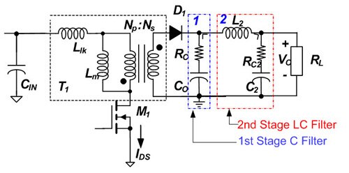
Figure 1: Flyback converter using 2nd stage LC filters.
There are three popular ways to derive a small signal model for Flyback:
- State Space Averaging method introduced by Middlebrook;
- PWM switch modeling from Vorperian;
- Averaged Switch method from Robert Ericsson.
The State Space Averaging method has been used for modeling many PWM converters and has been proven to be a useful tool in designing a stable loop. However, since the State Space Averaging method utilizes the parameters like the current signal inside the inductor and the voltage across the capacitor, the derivation work must be redone if any other active components are added. This feature makes the State Space Averaging method not convenient to model the Flyback converter with 2nd stage LC filter.
The PWM switch modeling method linearizes the switching components into a small signal model. PWM switch modeling can be initiated once the circuit looks like Figure 2a. As shown in Figure 2(a), the Flyback converter is firstly configured into buck-boost by reflecting its secondary side to its primary side through impedance reflection. The three terminal PWM switch network (a-c-p terminals; active-common-passive terminals) in buck-boost can be replaced with already existing linearized models in either the CCM or DCM (Figure 2(b)) operating conditions. By plugging in these already derived linearized models, a small signal model of the Flyback converter power train is ready for finding the pole(s) and zero(es) in a closed loop.
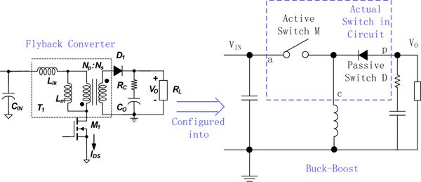
Figure 2(a): Configuring flyback into buck-boost.
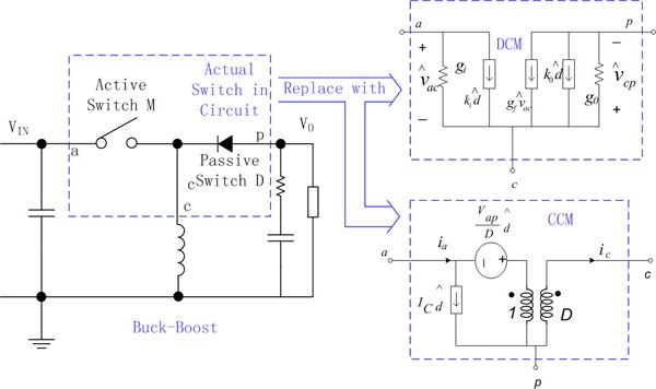
Figure 2(b): PWM switch modeling in buck-boost.
There are two ways of modeling a Flyback converter using the Averaged Switch method. One way is to reflect the load to the primary side and then replace the FET and diode with perturbed and linearized models as we did using a PWM switch. This approach seems less attractive since it takes extra effort to derive the Averaged Model while the PWM switch models are readily available for plug-in. The other way of modeling is to derive the Averaged Model directly without impedance reflections. However, the model derived using this approach is more complicated than the model derived using a PWM switch, which makes it not a good choice for modeling Flyback. Thus, the PWM switch modeling is the most efficient option for modeling a Flyback converter with 2nd stage LC filter. Compared to the more straight-forward PWM Switch method, both averaged switch methods require more steps or more complication to find the small signal model to find the pole(s) and zero(es) for flyback.
Impedance reflection described for PWM switch model for flyback
To use the PWM Switch method to analyze the stability and output set point tolerance issues introduced by a 2nd Stage LC output filter, one needs to do the impedance reflection to simplify the input to output model. To analyze the small signal model for a Flyback converter, start by reflecting the load and filtering caps (impedance) on the secondary side to the primary side.
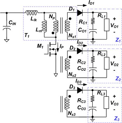
Figure 3: Flyback Converter with multiple outputs.
Figure 3 illustrates a simplified Flyback converter with three outputs. With the reflected impedance, a Flyback converter turns into a buck-boost Converter. Z1, Z2 and Z3 are the output impedances for the three outputs, respectively, and can be calculated as follows:

Recalling the basic operations for a Flyback converter, energy is transferred when the main switch M1 is turned off. The link between the primary side and the secondary side is the flux inside the magnetic core. This is illustrated in Figure 4.
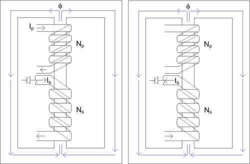
Figure 4: Current flow when switch M1 is on.
As shown in Figure 4(a), for a single output configuration with switch M1 on, current Ip flows through the primary side winding as flux Φ increases. Since the diode is reverse-biased, there is no current flowing through the secondary side winding. When switch M1 is turned off, as shown in Figure 2(b), to keep the flux remain unchanged, the diode is now forward-biased and conducting. Then, the following equations apply:

Based on equation (9), the output impedance for each output can be reflected to the primary side by multiplying a coefficient and in parallel. With the reflected impedance, a Flyback converter turns into a buck-boost converter. A Flyback converter with multiply outputs can be simplified into a buck-boost with several loads in parallel, as shown in Figure 5.
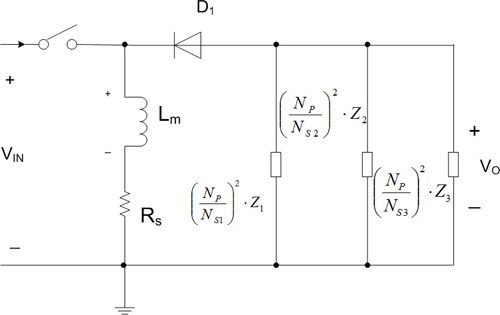
Figure 5: Simplified buck-boost converter with multiply loads in parallel.
With the loads reflected from the secondary side to the primary side, a Flyback converter can be analyzed as a buck-boost converter. This practice can greatly ease the analytical work for the applications in which second stage LC filters are used at each output for reducing output voltage ripple.
Transfer function derived for PWM switch model for flyback
Using the PWM Switch method to analyze the stability and output set point tolerance issues introduced by a 2nd Stage LC output filter, impedance reflection simplified the input to output model to a buck-boost (Figure 5). With reflected impedance simplification demonstrated above, a Flyback converter turns into a buck-boost converter for the next step. This simplification can greatly ease the analytical work for the applications in which a second stage LC filters are used at each output
Since the buck-boost converter operates in CCM and DCM depending on the load conditions, there are two different PWM switch models for the switch in CCM and DCM, respectively. Figure 6 shows the PWM switch in CCM while Figure 7 shows the PWM switch in DCM.
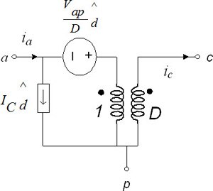
Figure 6: PWM switch in CCM.
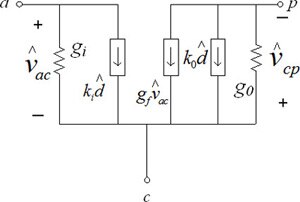
Figure 7: PWM switch in DCM.
The appropriate PWM switch model can be combined with the buck-boost converter depending on the operation mode(s) of the converter. Figure 8 shows the PWM switch in the converter while the converter runs in CCM while Figure 9 shows the PWM switch in the converter while the converter runs in DCM.
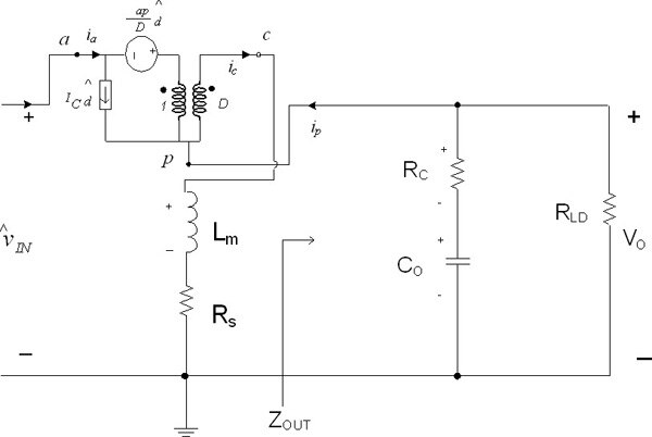
Figure 8: PWM switch in buck-boost in CCM.
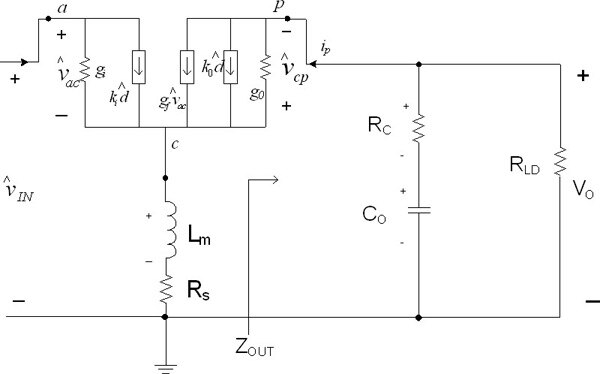
Figure 9: PWM switch in buck-boost in DCM.
With the combined PWM switch and buck-boost model, as shown in Figure 8 and Figure 9, deriving the transfer function of the buck-boost converter power stage is simplified.
To illustrate the modeling process, Figure 10 is drawn as shown below.
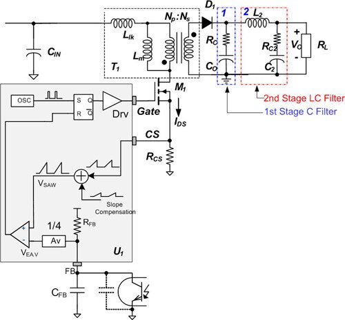
Figure 10: Flyback converter using 2nd stage LC filter with control circuit.
The model circuits with PWM switch plugged in are shown in Figure 11 and Figure 12.
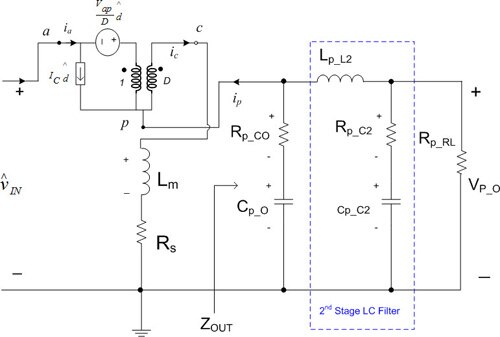
Figure 11: Flyback converter with secondary side components reflected to the primary side in CCM.
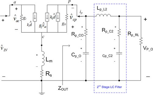
Figure 12: Flyback converter with secondary side components reflected to the primary side in DCM.

The transfer function from control to output voltage can be summarized as in (13). With the equation specified in (13), designers can optimize the system stability and the output regulation so that the best performance can be achieved by using the 2nd stage LC filter.
Rapidly create Flyback with 2nd stage output filter designs in minutes using Fairchild’s design tool and then save your designs for future reference. Fine-tune your design parameters without a bench prototype, swap component choices and perform detailed simulations and analyses.
Fairchild Semiconductor offers a wide variety of parts for that could fit into a multitude of applications. Check out their part offerings to determine if they have the solution to your application design requirements.
References
- Fundamentals of Power Electronics, Robert W Erickson Dragan Maksimovic
- Simplified analysis of PWM converters using model of PWM switch. II. Discontinuous conduction mode. Vorperian, V, Aerospace and Electronic Systems, IEEE Transactions, May 1990, page 497-505.
- Simplified analysis of PWM converters using model of PWM switch. Continuous conduction mode. Vorperian, V, Aerospace and Electronic Systems, IEEE Transactions, May 1990, page 490-496.
- Simplified analysis of PWM converters operating in discontinuous conduction mode using alternate forms of the PWM switch models, Jun Chen ; Ngo, K.D.T., Proceedings of the IEEE, Publication Year: 2000 , Page(s): 505 - 509
- Modeling the switch of PWM convertors (comments, with reply, on `Simplified analysis of PWM converters using models of PWM switch' by V. Vorperian), Aerospace and Electronic Systems, IEEE Transactions on Volume: 28 , Issue: 3 DOI: 10.1109/7.256319 Publication Year: 1992 , Page(s): 921-925.
- Averaged switch modeling of boundary conduction mode DC-to-DC converters. Jingquan Chen; Erickson, R.; Maksimovic, D. Industrial Electronics Society, 2001. IECON '01. The 27th Annual Conference of the IEEE Volume:2, DOI: 10.1109/IECON.2001.975867 Publication Year: 2001 , Page(s): 844-849 vol.2

免责声明:各个作者和/或论坛参与者在本网站发表的观点、看法和意见不代表 DigiKey 的观点、看法和意见,也不代表 DigiKey 官方政策。


