RL78/G14
Through Renesas RL78 CPU core, the RL78/G14 achieves reduced system power consumption overall, and supports multifunctional consumer and industrial applications without requiring additional external components.
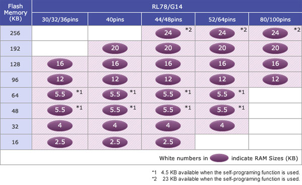
RL78/G14 Pin Count / Memory Size Lineup

Key Features
Operating voltage: VDD = 1.6 to 5.5 V
Max. frequency: 32 MHz
ROM capacities: 16 to 256 KB flash memory
RAM capacities: 2.5 to 24 KB
Data Flash: 4KB (16 to 64 KB Flash products), 8KB (96 to 256 KB Flash products)
Package:
- - 30-pin plastic SSOP (7.62 mm (300)), 32-pin plastic WQFN (fine pitch) (5x5), 32-pin plastic LQFP (7x7), 36-pin plastic FLGA (4x4), 40-pin plastic WQFN (fine pitch)(6x6), 44-pin plastic LQFP (10x10), 48-pin plastic LQFP (fine pitch) (7x7), 48-pin plastic WQFN (7x7), 52-pin plastic LQFP (10x10), 64-pin plastic LQFP (12x12), 64-pin plastic LQFP (fine pitch) (10x10), 64-pin plastic FLGA (5x5), 64-pin plastic LQFP (14x14), 80-pin plastic LQFP (fine pitch) (12x12), 80-pin plastic LQFP (14x14), 100-pin plastic LQFP (fine pitch) (14x14), 100-pin plastic LQFP (14x20)
Minimum instruction execution time can be changed from high speed (0.03125 µs: @ 32 MHz operation with internal high-speed oscillation clock) to ultra low-speed (30.5 µs: @ 32.768 kHz operation with subsystem clock)
General-purpose register: 8 bits x 32 registers (8 bits x 8 registers x 4 banks)
On-chip internal high-speed oscillation clocks
Selectable from 64 MHz (TYP.), 48 MHz (TYP.), 32 MHz (TYP.), 24 MHz (TYP.), 16 MHz (TYP.), 12 MHz (TYP.), 8 MHz (TYP.), 4 MHz (TYP.), and 1 MHz (TYP.)
On-chip single-power-supply flash memory (with prohibition of block erase/writing function)
Self-programming (with boot swap function/flash shield window function)
On-chip debug function
On-chip power-on-reset (POR) circuit and voltage detector (LVD)
On-chip watchdog timer (operable with the dedicated internal low-speed oscillation clock)
Multiply/divide/multiply & accumulate instructions are supported.
On-chip key interrupt function
On-chip clock output/buzzer output controller
On-chip BCD adjustment
I/O ports: 26 to 92 (N-ch open-drain: 2 to 4)
Timer
- 16-bit timer: 8 to 12 channels (TAU: 4 to 8 channels, Timer RJ: 1 channel, Timer RD: 2 channels, Timer RG: 1 channel)
- Watchdog timer: 1 channel
- Real-time clock: 1 channel (Correction clock output)
- Interval timer: 1 channel
Serial interface
- CSI
- UART/UART (LIN-bus supported)
- I2C/Simplified I2C communication
Different potential interface: Can connect to a 2.5/3 V device when operating at 4.0 V to 5.5 V
8/10-bit resolution A/D converter (VDD = EVDD =1.6 to 5.5 V): 8 to 20 channels
Standby function: HALT, STOP, SNOOZE mode
On-chip D/A converter
On-chip comparator
On-chip data transfer controller (DTC)
On-chip event link controller (ELC)
Operating ambient temperature: TA = -40 to +85°C
Key Applications
- Consumer Electronics, Industrial
|
Renesas Part Search
RL78 Family Microcontrollers
|


