Lattice Semiconductor 携手 NVIDIA 助力 AI 设计快速启动
当今 AI 模型竞赛如火如荼,功能日益强大,产品层出不穷,作为旁观者,可谓是乱花渐欲迷人眼。我们可以坐等最终胜者出现,再决定如何使用它们,但对于产品设计人员而言,这将是战略失误。他们应把握良机,将模型预测转化为实用、可信赖且具有实际价值的应用。
Lattice Semiconductor 与 NVIDIA 的合作,标示着 AI 时代产品设计理念的转变。双方通过一个 Sensor Bridge 参考设计,将传感器到 AI 流水线进行了标准化,从而降低了构建能够近乎实时感知、解读和响应的系统的门槛。现在,应用可以按照更加模块化的方式进行组装,从而加速开发进程,并催生出更智能、响应更迅捷的产品。
随着智能计算向数据产生的源头靠近,制约因素已从构建更好的模型,转变为如何设计这些模型在嵌入现实系统后的行为模式。系统关注什么、优先处理什么、忽略什么,这些将成为决定“AI 产品”是否被视作可靠、可预测且有用的关键设计参数。
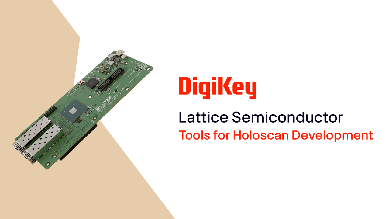
设计人员可以利用 Lattice Semiconductor 的 LF-SNR-ETH-EVN 来实现此参考设计(图 1)。这是一块基于 CertusPro-NX 的传感器到以太网桥接板,能够将异构传感器信号转换为标准化、低延迟的以太网数据流,供下游边缘 AI 系统使用。
 Lattice Semiconductor 的 LF-SNSR-ETH-EVN 获取来自异构传感器的输入,并将其转换为可供 NVIDIA 边缘模块处理的快速、结构化数据流。(图片来源:Lattice Semiconductor)
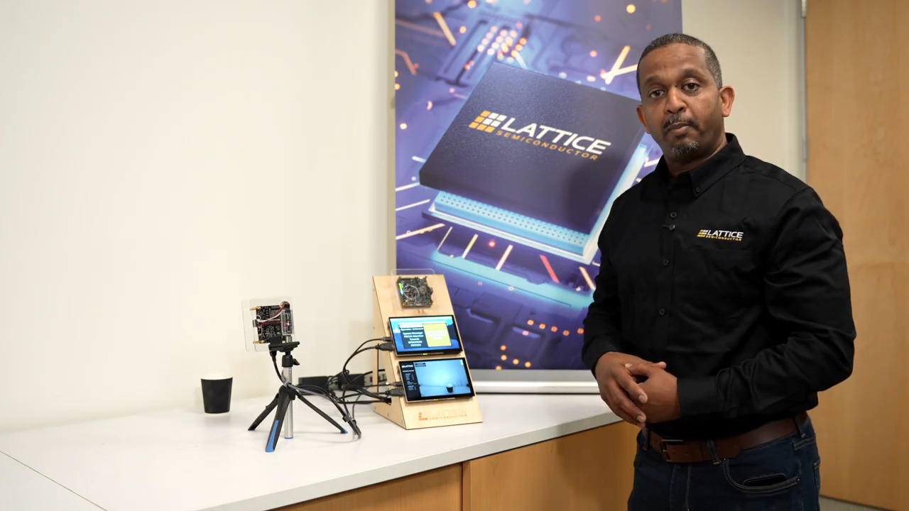
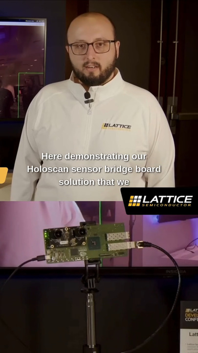
这个基于低功耗 FPGA 的硬件平台部署在边缘侧,其功能是将各种底层传感器信号转换为快速、结构化的数据流,以便通过以太网进行实时处理。它摄取原始传感器数据,对数据进行规范化和数据包化,并以低延迟、高吞吐量的方式将其传输给强大的图形处理单元进行处理。
Lattice 的开发板与 NVIDIA Holoscan Sensor Bridge 和边缘计算模块集成在一起,为实时传感器 AI 系统提供了一个完整的端到端栈。此项协作使得集成新传感器并将数据高效移入边缘 AI 平台(如 NVIDIA 的 IGX Orin 和 AGX Orin)上的 AI 推理流水线变得更加容易。
这种方式将云转变为支持性角色,聚焦模型训练、跨部署数据汇总以及管理更新和长期系统优化,而边缘模块则可专注于实时感知、解读和响应。
创建传感器到 AI 的设计
设计人员可以专注于快速构建“传感器到 AI”系统,并优化数据从物理信号到 NVIDIA 推理栈的流动方式。他们无需依赖模拟输入或关于系统行为的抽象假设,而是可以通过流经实际工作流水线的实时传感器数据来快速建立体验原型。
例如,设计人员可以从一个真实的传感器设置(如工业传感器或摄像头)开始,其数据流经 CertusPro-NX 桥接板,通过以太网传输,最终送达在边缘硬件上运行的、基于 Holoscan 的应用,进行实时 AI 推理处理。传统上,添加一个新传感器会引发大量工程工作,例如编写定制驱动程序、处理内核级集成、构建专门的数据流水线,仅仅是为了将信号转换为可用形式。Holoscan 通过标准化的 API 和传输层,降低了在边缘持续处理传感器数据的负担。
传感器数据被更统一地视为实时数据流的一部分,从而更容易将新数据源集成到现有的 AI 流水线中,而无需重构整个应用架构。
翻译层
基于 Lattice FPGA 的开发板,充当了物理世界与系统其他部分之间的可编程翻译层,从而减少了每次引入新传感器时重新设计硬件的需求。它包含了预配置的 FPGA 功能块,用于处理和适配传感器数据,以及完整的软件栈,用于在 NVIDIA 边缘 AI 硬件上收集、传输和处理这些数据。
这种方法将传感器集成从一项硬件限制转变为一个可配置的设计决策,随着产品需求的演变,极大地增强了系统的灵活性。设计团队可以在开发过程中无缝集成新传感器或增加额外输入,而无需对整体架构进行大规模重构。
在完整的生产系统投入运行前修改产品行为的能力,减少了定制集成工作,并允许在系统检测、动作触发和不确定性处理方面进行迭代改进。
结语
产品设计人员不能等待 AI“模型大战”尘埃落定。现在正是打造能够感知、决策并根据实时现实世界输入采取行动的 AI 驱动型应用的绝佳时机。Lattice Semiconductor 与 NVIDIA 的合作为设计人员提供了超低延迟的数据流水线,能够在更多领域催生出全新类别的 AI 应用。
关于此作者

Pete Bartolik 是一名自由撰稿人,二十多年来一直从事有关 IT 和 OT 问题及产品的研究和写作。他曾任 IT 管理刊物《计算机世界》的新闻编辑、一家终端用户计算机月刊的主编和一家日报的记者。

Have questions or comments? Continue the conversation on TechForum, Digi-Key's online community and technical resource.
Visit TechForum此作者发布的其它博客