Understanding the Cause of Fading in High-Brightness LEDs
投稿人:电子产品
2012-02-21
High-brightness LEDs tend not to burn out rapidly. Rather, they slowly fade away. A carefully designed LED lighting system can see the light source last for up to 50,000 or even 70,000 hours before the illumination is no longer sufficient for the intended job.
What causes the chip to lose luminosity, and can anything be done to arrest the decline? This article reviews the physics behind an LED’s photon generation to explore what happens when the device is new, and then why the performance inevitably deteriorates as the chip ages.
The author will also discuss what design engineers can do to maximize the longevity of the LED in their next design and casts an eye over what major LED suppliers such as Cree, OSRAM, and Seoul Semiconductor are doing to improve the next generation of commercial products.
Basic properties
Constructing an LED is relatively simple; choose appropriate n- and p-type semiconductors, bring them together to form a p-n junction or diode, connect the n-type to the negative terminal of a power supply and the p-type to the positive, and wait for things to start glowing.
The n-type semiconductor contains free electrons, while the p-type has electron vacancies or “holes.” The electrons and holes carry opposite charges and, under the bias voltage, migrate to the junction between the two materials where they can recombine. That recombination (sometimes) releases light in the visible part of the spectrum in a physical phenomenon known as electroluminescence.
That is the simple explanation, but, of course, the reality is a little more complex. To understand why an LED’s light output diminishes over time, it is necessary to delve a little more deeply into the physics.
Semiconductors are characterized by a level of conductivity that falls somewhere between metals and insulators. Conductivity in materials is governed by the “band gap.” The band gap is the energy differential between electrons that are constrained to the outer shells (or outer “orbits”) of the parent atoms (the valence band) and those that have gained sufficient energy (usually by thermal excitation) to escape the parent atom to become mobile and hence free to act as charge carriers (the conduction band).
Metals have virtually no band gap so there are many free electrons and the materials are good conductors. Insulators have wide band gaps severely restricting charge carriers. Semiconductors fall between the two. Silicon, for example, is a relatively poor conductor at room temperature, but things improve rapidly as the temperature rises and enough electrons gain the energy needed to jump the band gap.
The electrical properties of the various types of semiconductors are typically modified to make them more practical for use in electronic components by “doping” with other elements, such that more free electrons (or alternatively holes) are introduced to the base material. This improves the conductivity at a given temperature compared with the un-doped, so-called intrinsic semiconductor.¹
In an LED, near the p-n junction, electrons in the n-type material conduction band can “drop” into holes in the p-type valence band by emitting energy corresponding to the energy differential across the band gap. If the energy is released as a photon, its energy (and hence wavelength and color if in the visible part of the electromagnetic spectrum) corresponds to the band gap (Figure 1).

Modern white LEDs are based on indium gallium nitride (InGaN), deposited on a transparent substrate such as sapphire or silicon carbide (SiC). The band gap of InGaN can be manipulated by altering the ratio of GaN to InN such that emitted photons are in the 390 to 440 nm part of the spectrum (ultraviolet, violet-blue, and blue). “White” light is emitted because some of the blue photons are absorbed by the LED’s phosphor coating and are re-emitted as yellow. The combination of blue and broadband yellow produces white light (see the TechZone article “Whiter, Brighter LEDs”).
Less than perfect
Wafer fabrication is a tricky business, and no matter how skilled manufacturers become, it is impossible to produce LED dies that are free of defects in the bulk crystal lattice. During manufacture, so-called threading dislocations occur – these are minute discontinuities in the otherwise regular crystal structure. Threading dislocations are vertical micro-cracks caused by strain generated by the mismatch in InGaN and Sapphire or SiC crystal lattices (Figure 2).

Figure 2: Threading dislocations in InGaN substrate.²
Threading dislocations are a major problem for an LED designed with high efficacy in mind because recombinations between electrons and holes that occur at such sites are primarily “non-radiative.” In other words, no photon is emitted. This is because the dislocations introduce extra band gaps beyond the one that the designer intended, and hence do not correspond to the energy differential that produces a visible photon. In this case, energy is transferred by the emission of a “phonon,” a vibration introduced to the crystal lattice that adds nothing to the chip’s luminosity. Unfortunately, InGaN suffers from threading dislocations more than most other semiconductors, exhibiting typical densities exceeding 108 per cm².
Chipmakers suffer the threading dislocation deficiencies of InGaN because it has so many other properties that make it a good choice for LEDs. The material actually compensates somewhat for its own deficiencies by forming Indium-rich regions — these have a slightly lower band gap than surrounding regions — that tend to prevent diffusion of electron-hole pairs towards dislocations. The electron-hole pairs that recombine in these regions generate far more photons than those that occur near the dislocations. Nonetheless, the overall impact of threading dislocations is to lower the light output of a given LED.²
Why should a design engineer be overly concerned about defects introduced into an LED during its manufacture? After all, while accepting that the “quantum efficiency” (a measure of the percentage of electron-hole recombinations that produce a photon) is slightly reduced, the delivered device still performs to the manufacturer’s specifications. The answer is because things get worse over time, and the rate of degradation is directly related to the initial density of threading dislocations and the heat to which the LED is subjected.
Primary cause of failure
An LED is an electrical device, and as such there are many ways in which it can go wrong. (A previous article in TechZone — “Understanding and Preventing LED Failure” — discusses some of the manufacturing and packaging defects that can cause failure.) In practice however, LEDs are remarkably reliable and “failure” is most likely to be the result of light output falling below an acceptable threshold (typically 70 percent of the initial output (see the TechZone article “Determining LED Rated Life: A Tricky Challenge”). The primary cause of that fading (or “lumen failure”) is triggered (for the most part) by the minute threading dislocations introduced to the chip during wafer manufacture.
Threading dislocations act as nucleation sites for larger dislocations of the crystal. These form naturally due to heating during operation, thermal expansion and shrinkage when the LED is turned on and off, and mechanical stress such as vibration. As more and more dislocations occur over time, the number of sites for non-radiative recombination increases and quantum efficiency drops. (Some other factors, such as metal diffusion into the semiconductor from the connecting leads also contribute to lumen failure, but dislocations are the primary mechanism.)
The temperature to which the LED is subjected is a primary contributor to the rate of dislocation production. A hotter chip will form dislocations faster and hence fade quicker. This is a key reason why manufacturers advise keeping the chip’s junction temperature down. Figure 3 shows how operating life is influenced by temperature.

Figure 3: LED lifetime vs. junction temperature.
Worse yet, the non-radiative recombinations that cause vibrations of the crystal lattice add to the overall temperature. In other words, as the chip ages, it will run hotter and hotter for a given forward voltage due to an increased number of phonons, accelerating the formation of dislocations and the device’s eventual demise.
Greater numbers of dislocations have also been postulated to contribute to more rapid efficiency droop, a phenomenon whereby efficiency tails off with increased forward current (see the TechZone article “Identifying the Causes of LED Efficiency Droop”). However, more recent research suggests that this is not necessarily the case. While dislocations definitely lower peak efficacy, they can actually decrease the gradient of the efficiency droop curve after the peak efficiency point.³
More work ahead
Modern LED’s offer impressive longevity when operated at the manufacturers’ recommended forward voltages and junction temperatures.
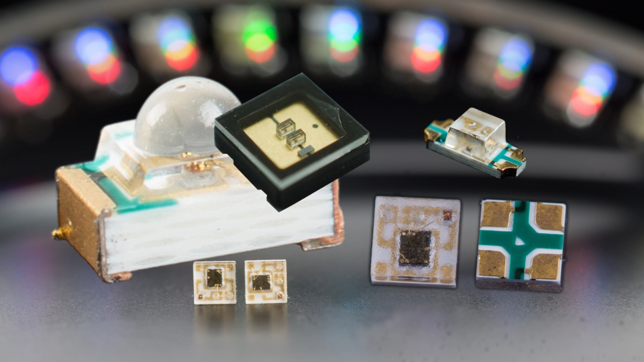
Chips such as Cree’s XT-E and XM-L high voltage white LEDs (Figure 4), OSRAM’s OSLON SSL devices (see for example the LA CP7P-JXKX-24), Lumex’s TitanBrite products, and Seoul Semiconductor’s Acriche chips can exceed operating lifetimes of 50,000 hours before luminosity drops below 70 percent of that when new. However, despite this good performance, the LED firms are not standing still.

OSRAM, for example, has sponsored some research at Germany’s Fraunhofer Institute for Applied Solid State Physics into alternative manufacturing techniques that promise to lower the density of threading dislocations in InGaN wafers. The work showed that an “ultra-low” dislocation GaN on sapphire exhibited a much reduced dislocation density of 8 x 10⁷ per cm², while a free-standing GaN substrate, where the GaN material is separated from the sapphire, had a threading dislocation density of 4 x 10⁷ per cm².4
For its part, Cree has just announced an addition to its XLamp range, the XB-D. Like the company’s other XLamp products, this device is based on Cree’s SiC technology. Although the company itself does not make too much fuss about the fact, other researchers have shown that InGaN LEDs deposited on SiC have a much lower threading dislocation density than those fabricated with sapphire.5
Seoul Semiconductor said it invests between 10 and 20 percent of its revenue on R&D, and has recently secured more than 10,000 patents in LED technology. Products such as the company’s Acriche range use InGaN LEDs fabricated using a novel process called metalorganic chemical vapor deposition (MOCVD). This patented technique, developed under the sponsorship of Seoul Semiconductor (among others), allows the fabrication of InGaN devices on sapphire with lower defect densities than other manufacturing techniques.6
In summary
The most common cause of failure for high-brightness LEDs is dimming over an extended period to the point that the light is no longer sufficient for its intended purpose. The primary cause of this loss of output is a reduction in quantum efficiency as dislocations in the chip’s crystal structure increase adding to the number of sites where non-radiative recombination can occur.
LED chipmakers are working hard to reduce the number of defects in the devices when new, but semiconductor manufacturing processes are not perfect and there will always some faults. The most important factor under the control of the design engineer that does influence longevity is junction temperature. Operating the LED according to the manufacturer’s thermal guidelines will reduce the rate of crystal degradation and ensure a long and bright operating life.
References:
- “Bonds, Bands, and Doping: How Do LEDs Work?” Rachel Casiday and Regina Frey, Department of Chemistry, Washington University.
- “The role of threading dislocations in the physical properties of GaN and its alloys,” J.S. Specka and S.J. Rosnerb, Materials Department, University of California, Santa Barbara, Hewlett-Packard Laboratories, Palo Alto.
- “Effect of dislocation density on efficiency droop in GaInN/GaN light-emitting diodes,” Martin F. Schubert, Sameer Chhajed, Jong Kyu Kim, and E. Fred Schuberta, Department of Electrical, Computer, and Systems Engineering, Rensselaer Polytechnic Institute.
- “Reduced non-thermal rollover of wide-well GaInN light-emitting diodes,” M. Maier, K. Koehler, M. Kunzer, W. Pletschen, and J. Wagner, Appl. Phys. Lett., vol. 94, no. 4, p. 041 103, Jan. 2009.
- “GaN-Based Electronic Devices,” Michael S. Shur.
- “Fabrication of nonpolar indium gallium nitride thin films, heterostructures and devices by metalorganic chemical vapor deposition,” Chakraborty Arpan.
免责声明:各个作者和/或论坛参与者在本网站发表的观点、看法和意见不代表 DigiKey 的观点、看法和意见,也不代表 DigiKey 官方政策。