Material and Manufacturing Improvements Enhance LED Efficiency
投稿人:电子产品
2013-01-15
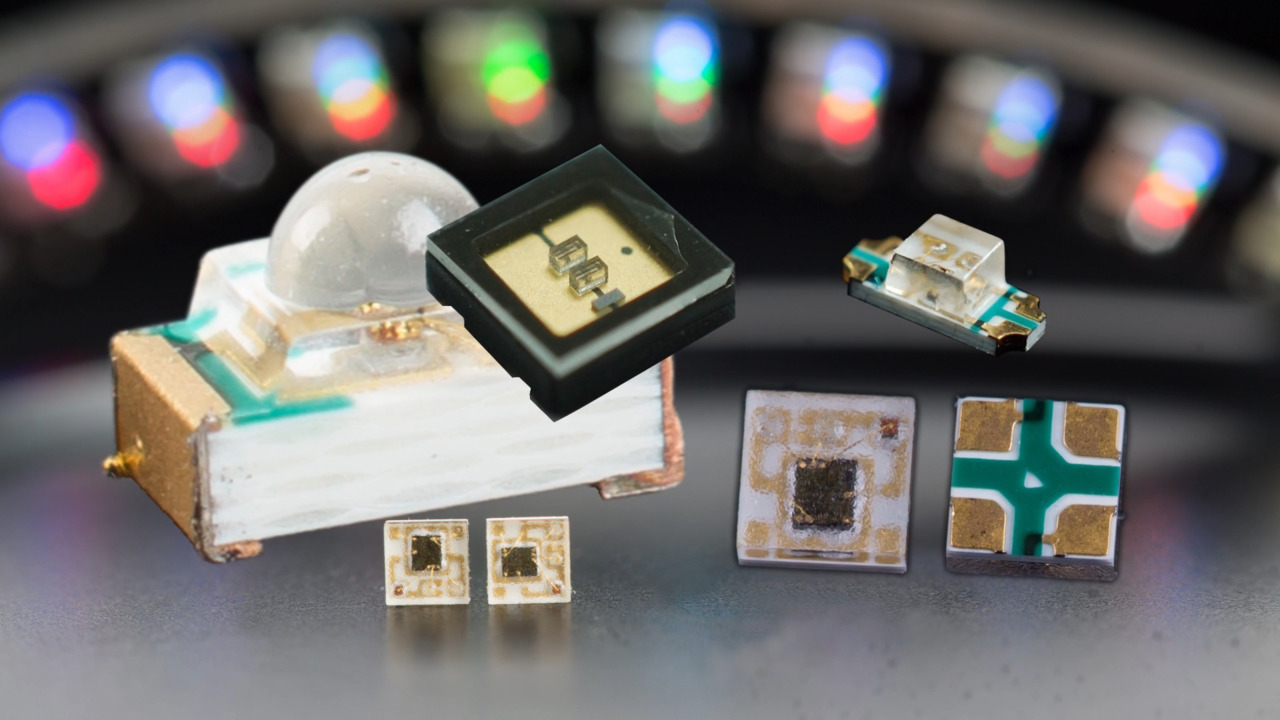
In theory, making high-brightness LEDs is easy. Just glue together n- and p-type semiconductors, add a small bias voltage, and stand back while the photons stream out. However, in practice these solid-state light sources are anything but simple. Advanced materials and manufacturing processes have come together to produce exotic devices with light outputs that would have been considered fanciful just half a decade ago.
Even though they produce impressive and highly efficient devices, the LED makers are not resting on their laurels. Leading LED companies such as Cree, OSRAM, and Seoul Semiconductor spend millions of dollars on material science and manufacturing technology to further enhance the performance of their products.
Contemporary high-brightness LEDs are already benefiting from advanced substrates and fabrication techniques, such as silicon carbide (SiC) and chemical vapor deposition (CVD), and tomorrow’s chips will take advantage of materials like patterned sapphire that are still percolating in the laboratory. This article takes a closer look at these materials and processes and assesses their impact on commercial LED performance.
Mind the band gap
Because the wavelength of the light emitted is a function of the energy band gap of the n- and p-doped semiconductor used to form the junction, engineers are limited in their choice of materials for fabricating LEDs. There is little point in selecting a semiconductor that emits photons that the eye cannot detect.
After many years of experimentation and hundreds of millions of research dollars, it turns out that Indium Gallium Nitride (InGaN) – a combination of Gallium Nitride (GaN) and Indium Nitride (InN) – is the best currently available semiconductor for high-brightness LEDs. The band gap of InGaN can be manipulated by altering the ratio of GaN to InN. The chips used at the heart of “white” LEDs, for example, emit photons in the 390 to 440 nanometer part of the spectrum (ultraviolet, violet-blue, and blue)1. These photons are then converted to white light by interaction with phosphor powder.
However, while InGaN has a number of advantages for photon generation, it does have some significant drawbacks from a volume manufacturing perspective. Chief among these is the fact that it is very difficult (and hence expensive) to “grow” InGaN ingots (unlike the silicon used for manufacturing integrated circuits (IC)). Ingots are advantageous for mass production because they can be sliced and processed as large wafers leading to lower cost chips.
Instead, manufacturers typically employ a much cheaper process whereby InGaN thin films are grown by a process known as epitaxy - the deposition of a crystalline overlayer on a crystalline substrate. There are several epitaxy techniques for forming the InGaN layer required for high-brightness LEDs, but the most common contemporary method is metal-organic CVD (MOCVD).
MOCVD is a complex process, but in basic terms, reactive gases are fed into a vacuum chamber and combine – at the atomic level – with the substrate and form a thin crystalline film.
During MOCVD, the crystalline structure of the deposited film attempts to orientate with the crystal structure of the substrate. The accuracy of this orientation depends on the similarity of the crystal lattice of each material. Poorly matched lattices result in a deposited film that while bulk crystalline on the macroscale is actually full of microscopic dislocations.
Reducing threading dislocations
A simplified schematic of the structure of a commercial high-brightness LED is shown in Figure 1.

Figure 1: Cross section of a high-brightness LED.
The MOCVD process builds up the LED’s active regions – the multiple layers sandwiched between the p- and n-contact – by depositing successive thin films typically on a sapphire substrate. Sapphire has a number of advantages as a substrate for LED production: it is relatively inexpensive; it is used as a substrate for ICs so manufacturing processes are well established; it is very hard and durable, and it is a good insulator.
But there are some drawbacks. One such drawback is the mismatch in the coefficient of thermal expansion between sapphire and InGaN that can lead to high stresses and cracking of the fabricated die. However, an even bigger drawback is the relatively large mismatch between the crystal lattice of InGaN and sapphire (Figure 2). The mismatch – of around 14.8 percent – results in microscopic flaws in the InGaN thin film known as threading dislocations (Figure 3).

Figure 2: Lattice mismatch between sapphire substrate and InGaN thin film creates threading dislocations. (Courtesy of Cree.)

Figure 3: Threading dislocations in InGaN substrate.
Threading dislocations are a challenge in the drive to improve LED efficacy because recombinations between electrons and holes that occur at such sites are primarily “nonradiative.” In other words, no visible photon is emitted. This is because the dislocations introduce extra band gaps beyond the one that the designer intended, and hence do not correspond to the energy differential that produces a photon with a wavelength in the visible part of the spectrum.
Alternatively, the energy emitted in the recombination is transferred by the emission of a “phonon”, a vibration introduced to the crystal lattice that adds nothing to the chip’s luminosity but does generate unwanted heat. Because of the mismatch with the sapphire substrate, InGaN suffers from many threading dislocations, exhibiting typical densities exceeding 108 per cm2 or more.2 Worse yet, threading dislocations increase in number as the LED ages, further compromising luminosity (see the TechZone article “Understanding the Cause of Fading in High-Brightness LEDs”).
The drive for greater efficiency
Because of its fabrication advantages, the majority of manufacturers have been prepared to accept the threading dislocation compromise that comes with sapphire while improving their products’ efficacy by focusing on other aspects of LED performance.
LEDs such as OSRAM’s OSLON SSL, for example, can produce up to 108 lm/W (at 350 mA), a state-of-the-art performance, while fabricated on a sapphire substrate. In fact, over 90 percent of today’s high-brightness LEDs from most of the leading manufacturers are fabricated on sapphire substrates.3
As the efficacy returns from improving the other aspects of a LED’s performance – such as carrier injection efficiency, photon extraction, and phosphor conversion efficiency – begin to diminish, LED makers are turning their attention to alternative substrates.
One of those alternatives is silicon carbide (SiC). Like sapphire, SiC can be produced in bulk using fairly standard semiconductor manufacturing techniques. It also has the added advantage of a coefficient of thermal expansion that’s similar to InGaN, limiting stress buildup and die cracking. The primary disadvantages are high cost and patented manufacturing processes that require the payment of licensing fees.
Cree, a leading U.S.-based LED lighting maker, has – perhaps not surprisingly considering it owns many of the manufacturing patents – championed the use of SiC substrates for LED fabrication. The major advantage the material has over sapphire is a lattice structure that's much more closely matched to InGaN. By using SiC, the lattice mismatch with InGaN is reduced to 3.4 percent.4 This close matching is still not sufficient to eliminate threading defects completely (Figure 4), although the defect density is considerably reduced – by at least one and sometimes two orders of magnitude lower than sapphire5 – dramatically decreasing the number of sights for nonradiative recombination, improving efficacy and prolonging the life of the LED by slowing the rate of fading.

Figure 4: Although threading defects still occur within InGaN-on-SiC substrates the defect density is considerably reduced compared with InGaN-on-sapphire.
Cree manufactures many of its LED products on SiC substrates. The XLamp XB-D series, for example, is built on the company’s “SC3” technology that features InGaN-on-SiC substrates. The XLamp XB-D offers an efficacy of up to 136 lm/W (at 350 mA) and can produce up to 289 lm at 1 A.
Both sapphire and SiC suffer from another significant drawback. The MOCVD process – whereby thin films are grown on a bulk crystal substrate – encourages the production of a polarized form of InGaN. Unfortunately, this polarization does nothing to help an LED’s efficiency, because as the current through the device increases, it induces an electric field in the crystal that starts to repel the very electrons and holes that should be combining to release photons. This is postulated as one reason why LEDs exhibit high efficacy at low currents, but the efficacy “droops” as the current increases (see the TechZone article “Identifying the Causes of LED Efficiency Droop”).
The solution, developed by South Korean LED maker Seoul Semiconductor, is simple in concept, but so difficult to put into practice that it has taken the company ten years to commercialize the technology.
What Seoul Semiconductor’s engineers have done is eliminate the polarization of InGaN-on-sapphire or on SiC by eschewing epitaxy and growing a bulk form of InGaN crystal from scratch. No substrate is required and the resultant bulk crystal can be sliced in a preferred direction to maximize the non-polarity.
As noted previously, growing bulk InGaN is very difficult and expensive. Seoul Semiconductor claims it is worth it, however, because the resultant “nPola” LEDs are five-to-ten times brighter than equivalent sapphire/polar InGaN devices. That means an engineer can use fewer chips in a lighting feature mitigating some of the initial higher cost (Figure 5).

Figure 5: Seoul Semiconductor’s nPola LEDs (right) are brighter than conventional devices so fewer are required in a light fixture.
These “nPola” LEDs are not yet available for commercial use, but will be soon. In the meantime, Seoul Semiconductor does offer a range of state-of-the-art devices such as its Z-Power P4 LEDs. These chips can provide up to 100 lm at a forward current of 350 mA.
Enhancing sapphire
Despite its higher threading defect count and the fact that it encourages InGaN to form polar crystals, there is plenty of life in sapphire substrate yet. LED manufacturers are looking at new ways to maximize the material’s potential. One technique under investigation is to produce so-called patterned sapphire. This technique forms a series of dome-like structures in a grid pattern on the sapphire wafer (Figure 6). The LED is then formed in a conventional manner on top of the sapphire substrate.

Figure 6: Patterned sapphire substrate with dome diameter of roughly 3 μm and spacing of roughly 2 μm.
For complex physical reasons, it turns out that the patterned substrate enables growth of InGaN layers with fewer threading defects that in turn does help improve the LED’s internal quantum efficiency (IQE).6 However, the IQE improvement is actually marginal, and the main gain from patterned sapphire is a marked increase in the ability of emitted photons to escape from the LED (extraction efficiency). For more information, see the TechZone article “Improving the Efficiency of LED Light Emission”.
Higher domes amplify the effect on the extraction efficiency (Figure 7). As yet, no manufacturer has adopted patterned sapphire substrates for their commercial devices, but it is surely only a matter of time before products are launched.
 intensity")
Figure 7: Electroluminescence (EL) intensity for different sapphire pattern heights as a function of forward current.
Summary
Several options are available to manufacturers looking to develop higher-efficacy LEDs, but each brings its challenges.
Exotic materials like nonpolar bulk InGaN, for example, promise the highest efficiency, but high cost, unconventional manufacturing techniques, and patent issues may prevent rapid adoption.
Previously, SiC substrates also fell into this category, but licensing agreements and higher volume production has driven down prices to make it a more commercially viable option with attractive properties.
SiC is still not cheap and many leading manufacturers consider the lower efficiency of sapphire is a worthwhile trade-off against a much reduced fabrication cost. Intensive research into the properties of this popular alternative is ensuring that its performance continues to improve.
While current leading high-brightness LEDs boast efficacies of over 120 lm/W, the theoretical maximum for a solid-state device is around 260 lm/W. So the substrate war has some time to run and it is highly likely that newer materials – yet to be synthesized – will enter the race to be the foundation upon which all future LEDs are based.
References:
- “Bonds, Bands, and Doping: How Do LEDs Work?” Rachel Casiday and Regina Frey, Department of Chemistry, Washington University.
- “The role of threading dislocations in the physical properties of GaN and its alloys,” J.S. Specka and S.J. Rosnerb, Materials Department, University of California, Santa Barbara, Hewlett-Packard Laboratories, Palo Alto.
- “SiC, sapphire and GaN materials status into Opto and RF businesses,” Dr. Philippe Roussel, April 2006.
- “Substrate-polarity dependence of metal-organic vapor-phase epitaxy-grown GaN on SiC,” T Sasaki and T Matsuoka, N I T Laboratories, Japan, November 1988.
- “Reduction of threading defects in GaN grown on vicinal SiC (0001) by molecular-beam epitaxy,” M. H. Xie,a) L. X. Zheng, S. H. Cheung, Y. F. Ng, Huasheng Wu, and S. Y. Tong, Applied Physics Letters, August 2000.
- “Characteristics of InGaN-Based Light-Emitting Diodes on Patterned Sapphire Substrates with Various Pattern Heights,” Sheng-Fu Yu et al, Journal of Nanomaterials, June 2012.
免责声明:各个作者和/或论坛参与者在本网站发表的观点、看法和意见不代表 DigiKey 的观点、看法和意见,也不代表 DigiKey 官方政策。