Solar Cell and Photovoltaic Primer
投稿人:电子产品
2011-06-30
There are many types of solar energy conversion devices currently on the market. They fulfill a wide range of roles from micropower applications like solar calculators and trickle charging for portable electronics, to utility-scale installations that provide tens or hundreds of megawatts to the electrical grid. At first, solar cell technology appears very straightforward, but it quickly becomes overwhelming with the wide range of cell types and materials. In this, the first of a series on what designers need to know about solar technology, we introduce some basics, beginning with a historical backdrop.
Photovoltaic cells come in many shapes and sizes. Solar power has a long history, and a great deal of the development can be traced back to the early days of space exploration. In space, the sun’s rays are not only abundant, but are also the only source of “on-site” power for orbiting vehicles. Of course, it’s always possible to lift other energy sources into space, but it is convenient to have a readily available source of power once you arrive.
Outside of aerospace, solar cells spent half a century as either a niche technology or something more suited to the science fair or other novelty application.
Energy crises and the green movement began to push photovoltaic technology much further in the last 10 years. Of course, the technology was advanced for use in space, but a completely different set of constraints closer to home sent researchers in new directions. Power density is the urgent criterion for space since it takes investments of millions of dollars per pound to launch anything into orbit. But down here, larger amounts of power are needed and economic factors like cost per watt are more important than pure performance.
Today, at least one exotic technology can trace its roots directly back to the aerospace industry: concentrator cells or concentrating photovoltaics (CPV). Although concentrating technology for utility-scale power production often depends on that old workhorse, the steam turbine, some installations use efficient photovoltaic cells at the focal point of mirrors or lenses. Efficiencies exceeding 40 percent are possible with these exotic materials, but the cost of the semiconductor materials is too high to cover large sunlight capture areas. Instead, mirrors or lenses focus the sun’s rays onto very small power conversion areas. Motorized multi-axis tracking equipment is also typical for these more costly cells to maximize the investment in the semiconductor material and the optics.
The two types of concentrator technology highlight the definitions for solar power conversion devices and photovoltaics. The two are often used interchangeably in the electronics and semiconductor industries because they’re more familiar to engineers in those fields. However, solar power can be used to generate heat that produces steam to drive a turbine as discussed above.
Cheaper materials were used in the early days of photovoltaics, but not for any seriously power-hungry application. The ability of standard silicon devices to produce a photoelectric current was actually a well-known phenomenon. To this day, test engineers regularly agonize over confusing measurement data before they realize the light on the microscope was left on while acquiring I-V data.
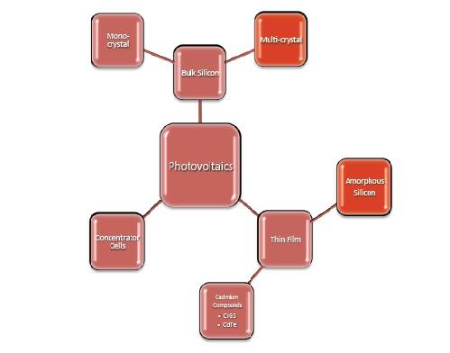
Broadly speaking, photovoltaic materials can be divided into two categories – crystalline and thin film. Crystalline varieties can include the exotic materials of the CPV arrays, but for most purposes, we are talking about silicon (Figure 1).

Figure 1: It’s a broad field of photovoltaic cell types, but generally speaking it can be divided into two categories – crystalline and thin film. Crystalline can include the exotic materials of the CPV arrays, but for most purposes, we are talking about silicon. (Source: Don Scansen)
Within the crystalline silicon category, there are several more device types. Higher-efficiency cells are possible using standard semiconductor-grade, bulk, single-crystal wafers. These are the most expensive but highest-performing type of silicon cell. In photovoltaic circles, this cell is known as monocrystalline silicon (c-Si).
Several manufacturing approaches try to take the crystalline silicon concept and make it cheaper to produce. Lagging only slightly in potential efficiency are the multi-crystalline cells. Growing ingots of multi-crystalline silicon not only requires less-fine control in the production process, it also allows wafers that are closer to square, which is obviously the ideal shape for improving the packing density of multiple cells within an array. Standard semiconductor-grade wafers are “squared off” to make them more packable, and this leads to waste material. Although these wafer bits can be recycled, the waste still adds to the cost, so many of the cost reduction methods are related to minimizing the material loss in producing the cells.
Multi-crystalline silicon (mc-Si) is cheaper to produce because it requires less process control and care than what is required to produce a single crystal. But the main feature is that these ingots do not have to be round. These cells are often also referred to as polysilicon, but that makes it too easy to confuse them with either the raw starting material supplied to any of the silicon crystal processes or the polysilicon (sometimes just poly) layer used for transistor gates in CMOS integrated circuits. The mc-Si bulk material is usually cast by careful cooling into a square shape. However, there is still the issue of slicing this ingot into cells, which consumes a significant volume of silicon.
To avoid this loss of input material, other manufacturing methods were sought that could still take advantage of bulk silicon’s relatively high conversion efficiency but with lower production costs. Enter string ribbon silicon, a process that allows pulling thin sheets of cell material from a melt. In addition to avoiding the waste from sawing a large block into thin wafer slices, the ribbon process allows added flexibility in setting the cell dimensions. Since the name of the game for solar power installations is creating a large capture aperture, continuous formation processes are a perfect fit.
The second large class of photovoltaic cell types is the thin-film variety. Rather than produce a cell from a block of essentially uniform material, the thin-film cell approach takes a large area substrate – typically glass – and coats it with the active layers. (Note: This is for illustration only since semiconductor junctions need to be formed to generate current from light and some cells are even multi-junction types, which layer different materials to widen the spectral range of absorbed light.)
Silicon is only one of a wide variety of materials deposited to form solar cells this way. Amorphous silicon (a-Si) thin-film cells take full advantage of the technology improvements and cost reductions that the LCD panel industry has driven for the last decade or more. Standard LCDs require extensive use of a-Si to create thin-film transistors to control each display pixel. The drive for ever-larger TVs helped to advance both substrate glass-making technology and silicon vapor coating systems to accommodate very large panels. The economies of scale in these giant glass panels are a major factor in the cost per watt that drives the economics of any large power-production installation.
You might think a-Si deposition would perform the best in terms of efficient use of starting material since the vapor coating onto the final glass substrate eliminates the usual dicing and slicing losses of the bulk solar materials. Unfortunately, there is a dramatic loss of the starting material – silane – during processing, which leaves less than a third stuck to the glass.
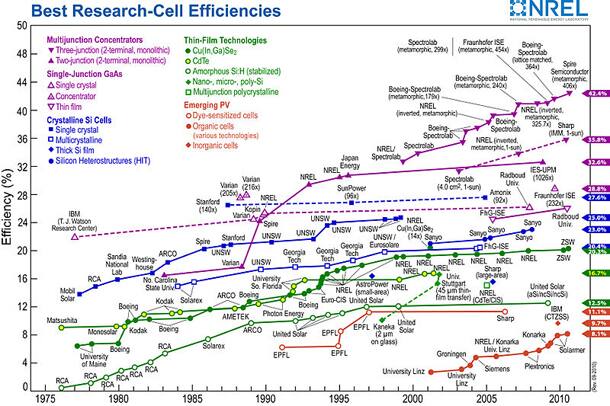
Although silicon enjoys the status of the material with the broadest knowledge base for high-volume manufacturing of any solar material, it is not the only choice for cost-effective thin-film cells with reasonably good or high efficiency (Figure 2). A few other thin film candidates are available that are not only cheaper to produce, but also offer better conversion efficiency than a-Si, even reaching the same 20 percent level of mc-Si. This material is widely known as CIGS− short for cadmium-indium-gallium-selenide.

Figure 2: Historical trends in efficiency records comparing the competitive solar cell types. Silicon offers competitive efficiencies for relatively low cost for a wide variety of applications.
It is interesting to consider that CIGS cells have not been around that long compared with their rivals since the photovoltaic effect was first observed in selenium almost 130 years ago. Selenium-based cells have come a long way since the 1 percent of Charles Fritts’ 1838 cell.
CIGS solar cells offer one of the very best combinations of high efficiency and low cost per watt of peak output. The drawback has always been the presence of cadmium and concerns over decommissioning and proper disposal or responsible recycling of the deadly material. But the benefits have prompted manufacturers to make recycling part of their up-front sales package.
CIGS cells take the cost-reduction possibilities of vapor deposition even further by avoiding the need for large-volume vacuum chambers like those required to produce device-quality a-Si. In one approach, CIGS cells are currently fabricated at standard atmosphere by coating the substrates with nanoparticles of the constituent materials and sintering them, a process that is far cheaper than anything requiring vacuum deposition chambers.
The key to the high-performing CIGS cell is the light spectrum it can absorb and convert into electrical current. It is a direct bandgap material, so a productive cell needs only a very thin layer of the active materials. Naturally, this reduces the cost of the cell.
The last major thin film solar cell is another cadmium based cell. Compound cadmium-telluride (CdTe) cells offer somewhat lower performance than their CIGS cousins. The best published cells offer efficiency just shy of 17 percent. CdTe makes up for the slight efficiency deficit with even simpler production processes. On the other hand, CdTe cells contain a much higher percentage of deadly cadmium.
For the most part though, silicon rules the photovoltaic world from calculators to residential rooftops to utility-scale solar farms. DigiKey itself specializes in silicon solar cells.
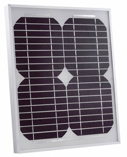
In comparing solar-cell varieties for larger-scale energy harvesting, it’s important to note that DigiKey offers several products appropriate for these applications. Parallax manufactures an 18-V, 10-W solar panel comprising four multi-crystalline silicon cells offering high output for a single panel as well as straightforward ganging of multiple panels for higher output. (Figure 3).

Figure 3: Parallax’s 18-V-at-10-W solar panel (DigiKey part # 750-00032-ND) comprises four multi-crystalline 340 X 280-mm multi-crystalline silicon cells. (Source: DigiKey)
免责声明:各个作者和/或论坛参与者在本网站发表的观点、看法和意见不代表 DigiKey 的观点、看法和意见,也不代表 DigiKey 官方政策。


