Securing MCU Designs
投稿人:电子产品
2013-10-30
In medical and military applications in particular, data security and the continued safe operation of the device are critically important. MCU manufacturers have built-in numerous features which, if used properly, often can detect and respond to device failure, as well as the presence of unauthorized code. This article will examine some of the hardware security features used by leading semiconductor vendors and their strategies for detecting and responding to abnormalities.

A secure system is basically one that cannot be copied, corrupted, or taken over by unauthorized parties. While this is usually thought of as a firewall or software problem, MCU manufacturers are increasingly building-in hardware safeguards that can help you prevent, detect, or at worst recover from attacks on your embedded system. Three aspects to security need to be considered in embedded designs:
- Confidentiality applies to information such as passwords or cryptographic keys that you cannot afford to have stolen. Hardware encryption modules can contribute substantially to data confidentiality.
- Integrity is essential for data being processed as well as the different components of the MCU, Flash memory in particular, and root tables and structures. MCUs have a variety of boot-up routines designed to check the integrity of on-chip memory as well as peripherals.
- Authenticity. If you cannot be assured of the integrity of data, at least be sure it is authentic, that is, it has not been changed by an attacker.
Virtually all MCUs at least check their operating integrity when first initialized or when recovering from a low-voltage condition. These checks occur during a power-on reset (POR) or brownout reset (BOR), though resets may also be triggered by access violations during normal operation. Some MCUs may do further system checks when starting up.
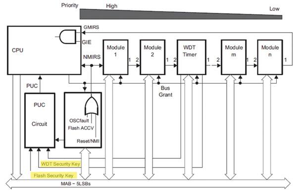
Texas Instruments’ MSP430 MCUs were one of the first to go for the ultra-low-power mantle. While not designed for heavily networked applications, the MSP430G2230IDR contains dedicated security features. The MSP430’s Flash-memory controller reports an access violation in response to any erroneous attempts to write to Flash. In addition, any write to an FCTLx register with any value other than 0A5h in the upper byte is reported as a security key violation. The same holds true for the Watchdog Timer. When the MSP430 is first powered up, or when VCC comes back up after a brownout event, a Power-On Reset (POR) signal is generated, which in turn generates a Power-Up Clear (PUC) signal. If the PUC results from a POR then the chip starts to initialize normally, activating the CPU and peripherals. However, if the PUC signal is generated by the Watchdog Timer or Flash-memory controller reporting a security key violation (Fig. 1), then the device is held in the reset state until the issue is addressed.
Memory protection
Detecting attempts to tamper with the Watchdog Timer or the contents of Flash memory is key toward preventing the takeover of an embedded system, or at least heading off data corruption. However, it is also possible to simply prevent attackers from gaining access to your boot code in the first place. The MSP430 contains a security fuse that protects code programmed into Flash memory.
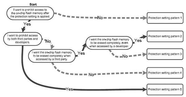
If third parties cannot read or write to the embedded Flash memory on an MCU, they are effectively prevented from tampering with the device. The Renesas RX631 provides multiple protection settings to prevent access to on-chip Flash memory by third parties (Fig. 2). They provide three types of protection:
- ID code protection—After the MCU is started in boot mode and a Serial Communications Interface (SCI) connection is established with a host device such as a PC, ID authentication is performed to prevent a third party from connecting and programming, reading, or erasing the on-chip Flash memory.
- On-chip debugger ID code protection—After the MCU is started in single-chip mode or user-boot mode and a connection is established with an on-chip debugger, ID authentication is performed to prevent a third party from connecting and programming, reading, or erasing the on-chip Flash memory.
- ROM code protection—When a PROM writer is used, third parties are prevented from programming, reading, or erasing the on-chip Flash memory.
Embedded developers need to develop a strategy to detect code that attempts to write to unallocated portions of memory. One approach involves filling in blank memory with undefined instructions. When illegal code attempts to access this memory it would then generate an Undefined Instruction Interrupt, alerting the CPU to take corrective action.
Microchip’s PIC24H MCUs provide both boot and program security (CodeGuard) for program Flash memory. PIC24H MCUs support Data RAM protection features that enable segments of RAM to be protected when used in conjunction with Boot and Secure Code Segment Security. When coupled with software encryption libraries, CodeGuard Security enables multiple parties to securely share resources (memory, interrupts, and peripherals) on a single chip.
When enabled, BSRAM (Secure RAM for Boot Segment) is accessible only from the Boot Segment Flash code and SSRAM (Secure RAM segment for RAM) is accessible only from the Secure Segment Flash code. Any attempted change to a restricted location in a protected segment causes a Security Reset.
Well ARMed
A high percentage of MCUs are based on ARM cores, which provide various hardware security features upon which chip vendors can build.
Larger MCUs may use the ARM® Cortex™-A-series processors, which include TrustZone security extensions. The TrustZone hardware architecture (Fig. 3) partitions both hardware and software resources so that they exist in two domains: the so-called Secure World for sensitive resources and the Normal World for all others. The two worlds communicate via the TrustZone-enabled AMBA3-AXI bus fabric, which creates a strong perimeter boundary between the two domains, ensuring that no Secure World resources can be accessed by the Normal World components.
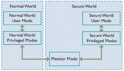
The TrustZone architecture enables a single core to run two virtual processors, one in each domain, via a context switch called Monitor Mode, access to which is tightly controlled to ensure the security of both domains. You can run a separate, secure operating system in the Secure World or just place a synchronous library of code there. It is also possible to implement a secure kernel that can run multiple, simultaneous Secure World applications, independent of what is happening in the Normal World.
The 536 MHz Atmel SAMA5D3 MCUs are Cortex-A5 based and incorporate 128 KB of RAM, 128 KB of Flash memory, and a high-data-bandwidth architecture. With its secure boot mechanism, hardware accelerated engines for encryption (AES, TDES) and hash function (SHA), the SAMA5D3 ensures anti-cloning, code protection, and secure external data transfers.
Being able to partition off two operating systems can provide excellent security, but going this route raises issues of cost, complexity, and code size. MCUs more commonly use Cortex-M-series processors, which are optimized for low-cost, low-power, mixed-signal embedded applications such as smart metering, automotive and industrial control systems, portable consumer products, and medical devices. Cortex-M4, Cortex-M3, and Cortex-M0+ MCUs include an optional memory protection unit (MPU) that provides fine-grain memory control, enabling applications to implement security privilege levels and separate code, data, and stack on a task-by-task basis. ARM licensees often implement additional security features.
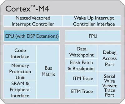
Cortex-M4 processors (Fig. 4) are the largest of the M-series line. For security, they provide an optional 8-region MPU. If access is made to an area of memory without the required permissions, a permission fault is raised, triggering a non-maskable interrupt (NMI) that initiates protective action by the RTOS or application code. The MPU is especially helpful for applications where some critical or certified code has to be protected against the misbehavior of other tasks.
In addition to an MPU, STMicroelectronics’ Cortex-M4-based STM32F2 MCU features a CRC calculation unit to verify data transmission or storage integrity. The CRC calculation unit helps compute a software signature during runtime, to be compared with a reference signature generated at link-time and stored at a given memory location.
Cortex-M3 processors are basically Cortex-M4s without DSP instructions and an (optional) floating-point unit. Texas Instruments’ Stellaris M3 line includes the Cortex-M3 MPU as well as system control block (SCB) registers that can only be accessed from privileged mode. In addition, the Flash memory controller (FMC) lets you apply Flash-memory protection on a 2 KB block basis.
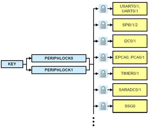
Silicon Labs’ Cortex-M3-based SiM3C167 Precision32 MCUs have a register lock-and-key mechanism that prevents any undesired accesses of the peripherals from firmware (Fig. 5). A key sequence must be written in order for the KEY register to modify any of the bits in PERIPHLOCKx. Any subsequent write to KEY will then inhibit any accesses of PERIPHLOCKx until it is unlocked again through KEY. If a peripheral’s registers are locked, all writes will be ignored. The registers can always be read, regardless of the peripheral’s lock state. The Product Training Module “Precision32 ARM Cortex-M3 MCU Introduction” provides more insight into the product.
The low-power Cortex M0+ processors also include the optional 8-region MPU available in its larger counterparts. Freescale’s Cortex-M0+-based Kinetis KL02 adds security circuitry to prevent unauthorized access to RAM and Flash contents. When Flash security is active, the SWD port cannot access the memory resources of the MCU.
NXP’s LPC4350 includes a Cortex-M4 processor and a Cortex-M0 coprocessor on a single chip. While the tiny Cortex-M0 is lacking in security features, the larger core takes up the slack. In addition to the MPU, the LPC4350 offers hardware to protect stored data content and to accelerate processing for data decryption, data integrity, and proof of origin. Its AES engine supports 128-bit ECB/CBC decode and CMAC hash calculation.
Summary
Device security is both a software and hardware problem, though one made easier by the presence of various MCU safety features. Taking advantage of them can result in safe operation in otherwise risky environments. For more information on the products discussed in this article, use the links provided to access product pages on the DigiKey website.
免责声明:各个作者和/或论坛参与者在本网站发表的观点、看法和意见不代表 DigiKey 的观点、看法和意见,也不代表 DigiKey 官方政策。


