Optimizing Sensor Data Acquisition in Industrial Automation
投稿人:DigiKey 欧洲编辑
2013-03-14
This article looks at the different data acquisition architectures and analog front-end devices that can be used for interfacing sensors in industrial automation applications. It covers the different bit widths, sampling requirements, settling times and the advantages of different data conversion techniques for different types of sensors. It also covers the AD7798 and LTC2389 successive-approximation converters from Analog Devices and Linear Technology, and the AD7788 and LTC2451 sigma delta converters as well as the Semtech SX8725, data acquisition system-on-chip.
Data acquisition in industrial automation applications can use several different types of converter, from successive-approximation (SAR), sigma-delta (∑Δ), and pipelined analog-to-digital converters (ADCs), but some are more suited to the needs of acquiring data from sensors.
While low power can be a key requirement in such an environment, speed of response is also important for feedback loops. Being able to interface easily to wireless sensor networks is also a key requirement to provide data that can help optimize the automation process and provide vital information on the health of equipment. This balance of power, accuracy, and speed provides the engineer with a complex design space. This can be tackled with individual components, from the ADC, with filters and programmable gain amplifiers to zoom in on the area of interest to speed up the data acquisition process to fully integrated system-on-chip devices.
Within this design space there are key choices around the type of ADC that is used. Data can be captured for a number of reasons in an industrial automation design – from sending data back to a controller for remote monitoring to implementing a feedback loop to control a process. As a result, industrial automation applications cover a range of devices with different resolution, sampling, and latency.
Successive approximation
The successive-approximation architecture (SAR) provides resolution from 8 to 18 bits, and sampling rates up to several megahertz (MHz). The data is generally output via a standard serial interface such as I²C or SPI, which works well with automation equipment, feeding the serial data to a microprocessor or wireless node.
In order to process the signal output from a sensor or amplifier, SAR ADCs have an input sample-and-hold (SHA) block to keep the signal constant during the conversion cycle. A key point is that the data corresponding to that specific sample is available at the end of the conversion time, with no pipeline delay or latency. This makes the SAR ADC easy to use in single-shot, burst-mode, and multiplexed applications, and works well for a sensor or bank of sensors that may take a sample every few seconds for monitoring applications. This may not be as well suited to feedback applications that need to control an actuator or heater, depending on the results of the sensor.
Calibration
Calibration has in the past been an issue with SAR devices. Switched-capacitor (or charge-redistribution) architectures have become popular at the heart of today’s CMOS-based SAR ADCs, as the accuracy and linearity come from the photolithography, which defines the capacitor plate area. This allows small capacitors to be implemented in parallel with the main capacitors, so that they can be switched in and out under control of auto calibration routines. This provides high accuracy and linearity without the need for more costly thin-film laser trimming.
These switched capacitor architectures also have good temperature tracking between the capacitors of around 1 ppm/°C, giving a high degree of temperature stability that is important for industrial environments.
Input multiplexing can be added to the basic SAR ADC function, allowing the integration of a complete data-acquisition system on a single chip. Additional digital functions such as multiplexer sequencing and auto calibration circuitry are also becoming common.
The internal conversion process of the SAR ADCs is controlled by a high-speed clock (internal or external, depending on the ADC) that does not need to be synchronized to the input, simplifying the system design.
Linear Technology’s LTC2389-18 is a low noise, high speed, 18-bit successive-approximation register (SAR) ADC that can be used for high performance data acquisition from sensors in industrial automation. It operates from a single 5 V supply and pin-configurable, fully differential (±4.096 V), pseudo-differential unipolar (0 V to 4.096 V) and pseudo-differential bipolar (±2.048 V) analog input ranges, allowing it to interface with multiple signal chain formats without requiring additional level translation or signal conditioning. This can dramatically simplify the design of the data acquisition system.
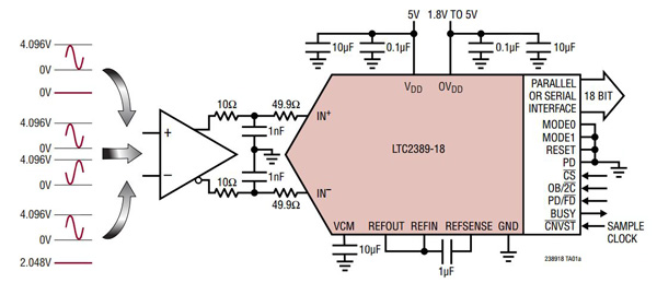
The LTC2389-18 achieves ±3 LSB INL (maximum), no missing codes at 18-bits, and 99.8 dB (fully differential)/95.2 dB (pseudo differential) SNR (typical). The family of devices is pin- and timing-compatible family from 250 kSPS to 2.5 MSPS and includes a precision 20 ppm/°C internal reference and reference buffer to reduce the number of external components required and save board space.
Similarly, the AD7988 family from Analog Devices is a 16-bit successive approximation ADC that operates from a single power supply, VDD. The AD7988-1 offers a 100 kSPS throughput, and the AD7988-5 offers 500 kSPS throughput. They sample an analog input between 0 V and the external reference voltage VREF, which can be set independently of the supply voltage, VDD. This gives the designer more flexibility in matching the input range to the sensor output regardless of the device voltage.
The SPI-compatible serial interface also features the ability, using the SDI input, to daisy chain several ADCs onto a single, 3-wire bus. It is compatible with 1.8 V, 2.5 V, 3 V, or 5 V logic by implementing the separate supply voltage (VIO).
The PulSAR architecture implemented in the devices uses internal switched capacitor techniques to extend the resolution of SAR ADCs to 18 bits and avoid the need for expensive thin-film laser trimming. The SAR algorithm takes two phases to determine the ADC output code. The first phase is the acquisition phase, where the SW+ and SW− are initially closed (see Figure 2). All the switches are connected to the IN+ and IN− analog inputs, thus each capacitor is used as a sampling capacitor acquiring the analog signal at the input. The second phase is the conversion phase where the SW+ and SW− are open. The inputs are disconnected from the internal capacitors and applied to the comparator inputs. This results in an unstable comparator. Without detailing the SAR algorithm, switching each element of the array between REF and REFGND, starting with the MSB, brings the comparator back into a balanced condition and thus generates the output code representing the analog input signal.
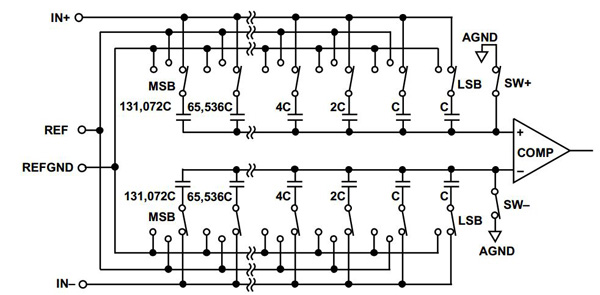
Figure 2: The input stage of ADI’s PulSAR successive approximation ADC.
Sigma-Delta converters
Sigma delta (∑Δ) ADCs are used for applications requiring high resolution (16 bits to 24 bits) and effective sampling rates up to a few hundred hertz, lower than the SAR devices. This high resolution, together with on-chip programmable-gain amplifiers (PGAs), allows the small output voltages of sensors such as weight scales and thermocouples to be digitized directly, reducing complexity and cost in many industrial automation designs.
This architecture also provides excellent rejection of 50 Hz and 60 Hz power-line frequencies with the right sampling rate and filter characteristics, a key advantage in industrial environments. ∑Δ ADCs offer an attractive alternative to traditional approaches using an instrumentation amplifier to boost the signal to be converted by a SAR ADC.
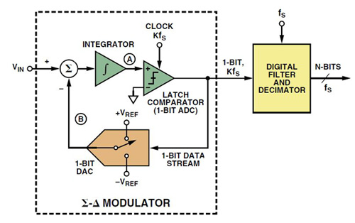
The idea behind the converter is the combination of a 1-bit ADC acting as a comparator, and a 1-bit DAC acting as a switch. The output of the converter core is a 1-bit stream of data and the ratio of the 1-s in the output stream to the total number of samples in any given interval is proportional to the DC value of the input, giving the result.
A key advantage for sensor design in industrial applications is that this approach also provides noise shaping by acting as a low-pass filter for the signal and a high-pass filter for the quantization noise. The digital filter is an integral part of the operation of the device and can be optimized to give excellent 50 Hz/60 Hz power-frequency rejection. One problem, though, is that this introduces pipeline delays, and this has to be considered carefully if the design includes a multiplexed front end. The best way to do this is to leave the filter to settle to a new value before the output data is read, which may take several clock cycles and slow down the acquisition time. However, this is unlikely to be an issue with a sensor design for industrial applications unless it is a high-speed image sensor. Other pipelined ADCs are more appropriate for that type of system.
A first-order, single-bit ∑Δ ADC is inherently linear, but does not provide sufficient noise shaping for high-resolution applications. By increasing the number of integrators in the modulator in the same way that poles are added to a filter, second and third order ∑Δ converters can provide higher resolution at the cost of more complex implementation.
Linear’s LTC2451C is a 16-bit, ∑Δ analog-to-digital converter that has a small footprint to fit into industrial designs. It uses a proprietary input stage to overcome several of the limitations of this conversion approach.
The device uses a single 2.7 V to 5.5 V supply, accepts a single-ended analog input voltage, and communicates through an I²C interface. The converter includes an integrated oscillator that does not require any external components, and uses a proprietary input sampling scheme that reduces the average input sampling current several orders of magnitude lower than conventional ∆∑ converters.
The device is capable of up to sixty conversions per second and, due to the very large oversampling ratio, has extremely relaxed anti-aliasing requirements. In the 30 Hz mode, the LTC2451 includes continuous internal offset calibration algorithms, which are transparent to the user, ensuring accuracy over time and over the operating temperature range.
Following a single conversion, the LTC2451 can automatically enter sleep mode and reduce its power to less than 0.2 µA. If the user reads the ADC once per second, the LTC2451 consumes an average of less than 50 µW from a 2.7 V supply.
At power-up, the LTC2451 is set to its default 60 Hz mode and performs a conversion. Once the conversion is complete, the device enters the sleep state and remains there while it is not addressed for a read or write operation, with the conversion result held indefinitely in a static shift register.
Once the LTC2451 is addressed for a read operation (hardwired at location 0010100), the device begins outputting the conversion result under the control of the serial clock (SCL) and there is no latency in the conversion result. The data output is 16 bits long and outputs from MSB to LSB, and the data is updated on the falling edges of the clock, allowing the user to reliably latch data on the rising edge.
The LTC2451 data output has no latency, filter settling delay, or redundant results associated with the conversion cycle, and there is a one-to-one correspondence between the conversion and the output data. This makes it suitable for multiplexing multiple analog input voltages, overcoming one of the issues with traditional ∑Δ architectures. In the slower 30 Hz mode, the device adds offset calibrations during every conversion but this is transparent to the user and has no effect upon the cyclic operation. All of this helps provide a more stable data conversion, particularly with respect to the temperature, which is vital for an industrial data acquisition application.
The proprietary input sampling scheme also reduces the average input current by several orders of magnitude when compared to traditional delta-sigma architectures. This allows external filter networks to interface directly to the device to reduce noise and spurious readings from the industrial environment. As the average input sampling current is 50 nA, an external RC low-pass filter, using a 1 kΩ and 0.1 µF, results in less than 1 LSB additional error.
The ∑Δ ADC is an attractive alternative when very low-level signals must be digitized to high resolution. However, the ∑Δ ADC is more digitally intensive than the SAR ADC, may therefore require a somewhat longer development cycle, and may not be suitable for an energy harvesting power source. Evaluation boards and software can greatly assist in this process.
ADI’s AD7788 is a low power ADC that combines the ΣΔ modulator with digital filtering for the measurement of wide dynamic range, low frequency signals, such as those in pressure transducers, weigh scales, and temperature measurement applications in industrial applications.
The output rate of the AD7788 (fADC) is 16.6 Hz with the settling time of 120 ms, and normal-mode rejection comes from the filter notches placed at both 50 Hz and 60 Hz with this update rate.
Sensor interfacing
Often though, the output signal of most sensors is less than ideal and low-cost sensors introduce quite a large spread of gain and offset variation into the production of a sensing device. A conventional way to overcome this spread is to add amplification ICs and to laser trim the amplification settings before connecting the sensing element to the ADC, or to buy higher cost, more sensitive, better-controlled sensor elements.
Semtech developed its ZoomingADC to overcome the gain and offset variations by combining the advantages of over-sampled ADCs with an embedded amplification stage to measure low cost sensor elements with the highest resolution.
Acquiring a sensor signal with a regular SAR ADC can mean a waste of resolution or a need for several external components that have to be adapted to the sensor, often through complex and costly calibration algorithms.
Most common sensors, such as temperature sensors or pressure transducers have relatively static signals, and the main challenge for the ADC is accuracy. This is best handled by over sampled ADCs, such as sigma-delta and incremental converters.
The first limitation of an ADC is the quantization error. This is a fundamental limitation of the ADC conversion process. The normal way to reduce this error is to increase the resolution of the ADC at the price of a longer acquisition time, a higher current consumption, and, most often, a more expensive bill of materials.
Take, as an example, a chemical sensor with a 5 V or less supply voltage and with an output varying from 1.15 to 1.25 V. Reading it directly with a 10-bit ADC will give a step of 5 mV, or a resolution of 20 points on its output. Amplifying its output by a factor of four will mean an output of 4.6 V to 5 V, boosting the resolution to 80 points. But by focusing on just part of that output voltage, the resolution can be increased to 1024 points using just a 10-bit ADC.
The ZoomingADC is the combination of a high-resolution ADC with several programmable gain and offset pre-amplifiers. The gain and offset settings can be made in very fine steps (10%) over a very large range (gain from 0.5 to 1000, offset can be set bigger than the signal input full scale).
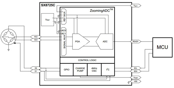
Figure 4: Semtech’s SX8725 sensor system-on-chip with ZoomingADC.
By sharing the gain and offset compensation over three stages, the ZoomingADC makes it possible to compensate for large offsets on small signals without saturation or resolution losses. An extra feature of the ZoomingADC is the capability to capture single and differential signals. The ZoomingADC is based on a differential signal path, and accommodates single-ended signals with the addition of a controlled offset.
The SX8725C is a data acquisition system based on Semtech's low power ZoomingADC technology. It directly connects most types of miniature sensors with a general-purpose microcontroller. With a 16-bit differential input, it can adapt to multiple sensor systems and the digital outputs are used to bias or reset the sensing elements.
The core of the zooming section is made of three differential programmable amplifiers (PGA). After selection of an input and reference signals VIN and VREF and the ADC combination, the input voltage is modulated and amplified through stages one to three. Fine gain programming up to 1000 V/V is possible. In addition, the last two stages provide programmable offset so that the signal is moved into the right area, although each amplifier can be bypassed, if needed. The output of the cascade of PGA is directly fed to the ADC, which converts the signal into a digital stream.
Like most ADCs intended for sensing applications, the ZoomingADC is an over-sampled converter that is also an incremental converter with bipolar operation (the ADC accepts both positive and negative differential input voltages). In first approximation, the ADC output result relative to full-scale (FS) delivers the quantity.
The zooming function is implemented with three programmable gain amplifiers (PGA). PGA1 provides coarse gain tuning while PGA2 provides the medium gain and offset tuning to zoom into a particular area of interest. For high linearity data acquisition, PGA3 is used for fine grain amplification and offset tuning.
All the amplifiers are controlled via the ratios of capacitors and the user has control over each PGA activation and gain, as well as the offset of stages two and three, to zoom into the area of interest on the data acquisition spectrum.
Conclusion
Several different types of data acquisition architecture can be used in industrial automation applications. Sigma delta converters have had higher resolution than successive approximation, but have been limited in their use for taking one-shot measurements. With newer device architectures, this is no longer an issue and ΣΔ converters are increasingly being used in sensing designs in industrial applications where the inherent 50 Hz and 60 Hz noise rejection improve the performance. At the same time, the converters have been integrated into more complex system-on-chip devices to simplify the design process and provide the engineer with the ability to zoom into the area of interest without having to build complex signal conditioning equipment.

免责声明:各个作者和/或论坛参与者在本网站发表的观点、看法和意见不代表 DigiKey 的观点、看法和意见,也不代表 DigiKey 官方政策。


