How and Why to Use PIN Diodes for RF Switching
投稿人:DigiKey 北美编辑
2016-12-28
Switching RF power in portable applications is challenging for electromechanical switches due to size, cost and speed considerations. While PIN diodes offer some unique advantages relative to other non-mechanical options such as CMOS switches and MEMS structures, they are difficult to design into a circuit unless their characteristics are clearly understood.
This article will introduce the challenge of RF switching and describe the basics of PIN diode operation. It will then show how to design with PIN diodes, before providing some real-world PIN diode examples to show how the technology is advancing.
The RF switching challenge
In many applications, it is necessary to switch the RF signal path to route and connect to different antennas, amplifiers, and filters. This need for more switching with higher performance is only growing with the development of MIMO, multiband wireless devices (5G), and other advanced technologies, especially for portable and battery-powered devices.
Since these switches must work into the gigahertz region and higher, nothing about them is simple: their design, their underlying technology, the layout on the PC board, or matching their performance to the application priorities.
Each of these technologies offers tradeoffs in key performance parameters such as bandwidth, insertion loss, isolation, switching speed, and power handling (Figure 1).
(Note: "hybrid" switches combine PIN diodes and FET-based components.)
| Solid state switches | Electromechanical switches | |||
|---|---|---|---|---|
| Pin diode | FET | Hybrid | ||
| Frequency range | from MHz | from DC | from kHz | from DC |
| Intersection loss | Medium (Roll off at low frequencies) | High (Roll off at high frequencies) | High (Roll off at high frequencies) | Low |
| Isolation | Good at high frequencies | Good at low frequencies | Good at high frequencies | Good across broad frequency range |
| Repeatability | Excellent | Excellent | Excellent | Good |
| Switching speed | Fast | Average | Average | Slow |
| Power handling | Low | Low | Low | High |
| Operating life | High | High | High | Medium |
| Power consumption | High | Low | Moderate | Current interrupt feature reduces current consumption |
| Sensitive to | RF power overstress, temperature | RF power overstress, temperature | RF power overstress, temperature | Vibration |
| Agilent switch examples | P9400/2/4 85331/2 |
U9397, U9400 | L series, 8710x/20x | |
Figure 1: The general attributes of RF switches based on solid-state components of PIN diodes, FETs, and hybrid devices as well as electromechanical implementations. (Source: Keysight Technologies)
Representative maximum and minimum levels for the three classes of solid-state switches cover a wide set of overlapping ranges as shown in Figure 2. There is widespread interest in using FET switches due to their IC design and ease of use, as well as the enormous demand for RF switches in smartphones, routers, and other applications. As a result, vendors are releasing many new FET devices with improved specifications, causing the comparative attributes and numbers in the tables to shift.
| PIN diode switches | FET switches | Hybrid switches | |
|---|---|---|---|
| Lower frequency limit* | 100 MHz | DC | 300 kHz |
| Upper frequency limit* | >50 GHz | >20 GHz | >20 GHz |
| *Typical. Based on performance requirements. | |||
Figure 2: Upper and lower frequency limits for the three groups of solid-state RF switch components. New products and enhancements mean these numbers are constantly in flux. (Source: Keysight Technologies)
PIN diode basics
A PIN diode behaves as a current-controlled resistor at radio and microwave frequencies. Like the conventional PN diode, it allows current flow in one direction when forward biased, but not in the other when it is reverse biased. This functionality is a simple and critical functional block of many circuits spanning DC to RF.
However, unlike the PN diode, the PIN diode has an "intrinsic" layer sandwiched between its P and N layers. While the device physics are complex, the result is a controllable switching action with a twist. When the PIN diode is forward biased it allows RF energy to flow, and when reverse biased it blocks RF energy. This is the basis for using the PIN diode in a wide variety of RF switch topologies.
The electrical model of the PIN diode looks like an inductor in series with a resistor when forward biased. When reverse biased, it looks like an inductor in series with a paralleled capacitor and resistor (Figure 3). The specific values of the passive elements in these models depend upon the PIN diode model.
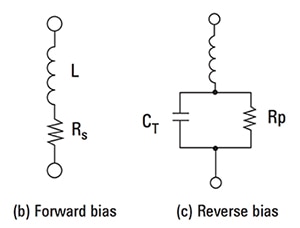
Figure 3: Model of the PIN diode when forward biased (left) and reverse biased (right) where Rs is the (low) resistance of the diode when forward biased; L is the parasitic inductance (largely a function of the package); CT is the sum of the diode junction capacitance and the parasitic capacitance of the package; and Rp is the (high) resistance of the diode when reverse biased. (Source: Keysight Technologies)
In general, PIN diodes offer very good linearity and can be used for very high frequency and high-power applications. Their downside is the large amount of DC power they need for biasing (the higher the DC power applied, the lower the insertion loss). Also, their isolation performance specifications are difficult to determine and they require carefully designed support circuitry.
Why PIN diodes are challenging to use
It’s a seemingly simple structure, which begs the question: Why is the PIN diode so challenging to use? The reason is simple. It’s a two-terminal device, and as such, the control port needed for biasing and the port for the RF signal are the same physical point. Thus, the design must allow them to "merge" at the diode, yet keep them isolated from the rest of the circuitry. As a result, engineers have mixed emotions about using PIN diodes since they are not the easiest switch option to use, but they can do things other options cannot.
Using the PIN diode
A diode alone is not a complete and useful switch as it is only the core switching element. At a minimum, an RF switch based on PIN diodes needs a DC blocking capacitor to prevent the DC bias current from reaching the RF output, and an RF choke to provide a path for the DC bias current to return while blocking the RF signal.
A basic single-pole, single-throw RF switch that can either pass or cut off an RF signal can be built using either a series or a shunt topology. The series approach provides minimum insertion loss over a broad frequency range (Figure 4). This configuration can function across a wide bandwidth, which is limited by the biasing inductors and the DC blocking capacitors. It can be expanded to a single-pole, double-throw configuration where the source signal can be routed to one of two ports.
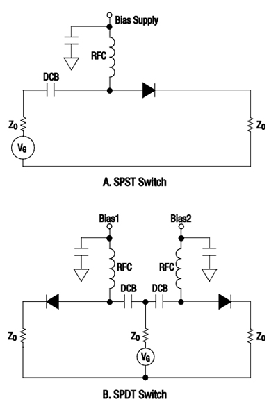
Figure 4: PIN diodes used in series mode for a) a basic SPST switch and b) an SPDT switch, where VG is the RF generator voltage. (Source: Skyworks Solutions, Inc.)
Similarly, shunt-diode switches can be used for basic SPST and SPDT functions (Figure 5). The shunt approach offers high isolation, and since the diode may be heatsinked at one electrode, it is capable of handling more RF power than a diode in a series topology. Some designs add a quarter-wave transmission line between the diode and its blocking capacitor to create lumped-series inductance for a low-pass filter. This enables the switch to work up to the desired frequency.
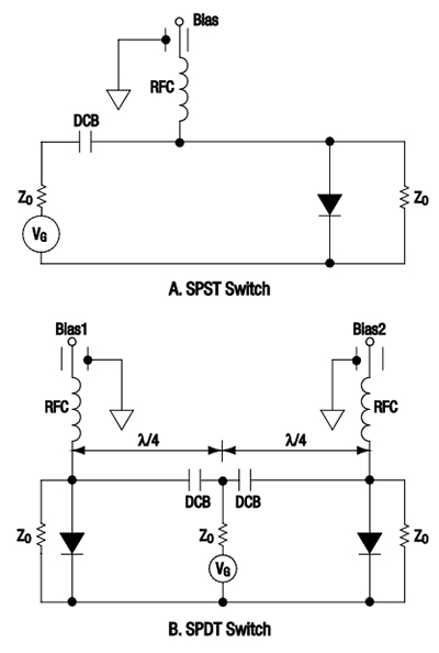
Figure 5: PIN diodes used in shunt mode for a) a basic SPST switch and b) an SPDT switch. Note the addition of quarter-wavelength transmission lines to form a low-pass filter. (Source: Skyworks Solutions, Inc.)
Using either a shunt or series topology, it is challenging to achieve better than 40 dB isolation using a single PIN diode, especially at the higher operating frequencies. These limitations can be overcome somewhat by using combinations of series and shunt diodes in what are called compound switches.
The PIN diodes are configured in either ELL (series-shunt) or TEE (shunt-series) topologies, (Figure 6). In a compound switch, the insertion loss state is when the series diode is forward biased and the shunt diode is at zero or reverse bias. For the isolation state, the reverse situation applies. Note that the bias circuitry of a compound switch is more complex than that needed in simple series or shunt switches.
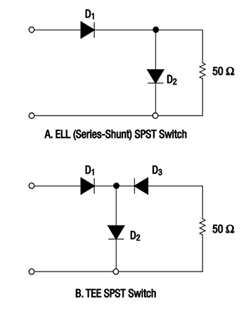
Figure 6: Use of series and shunt modes in compound topologies in a basic SPST switch to maximize desired performance while minimizing undesired specifications in both a) ELL and b) TEE configurations (support components not shown, for clarity). (Source: Skyworks Solutions, Inc.)
Another, more complicated approach to enhancing isolation performance uses a resonant structure to create a tuned switch (Figure 7). Here, two series or two shunt diodes are spaced a wavelength apart, yielding an isolation value 3 dB higher than a single diode switch can offer.
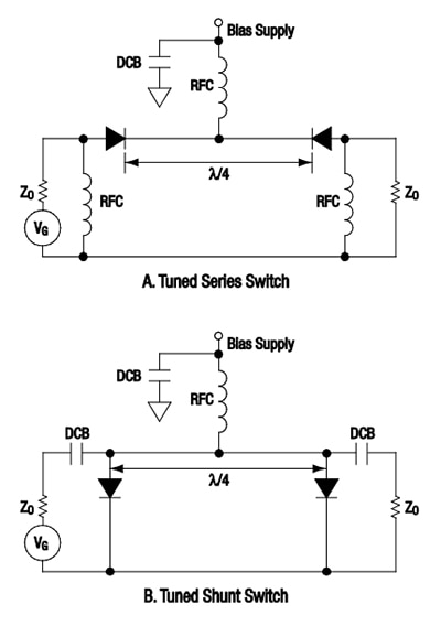
Figure 7: The resonant structure uses quarter-wavelength spacing between diodes as filter elements, and can be applied to create a tuned switch in both a) series and b) shunt modes. (Source: Skyworks Solutions, Inc.)
Biasing the PIN diode
The DC bias voltage needed to control the PIN diode's mode is a function of the diode as well as the RF signal level, temperature range, and other factors. This bias voltage must be decoupled from the RF signal and be stable, as any noise or ripple will affect the diode's operating point.
When used in high-power situations, PIN diodes need a high bias-control voltage to minimize the cross-modulating effects of the voltage swing of the RF signal. For example, a 100 W RF signal has a peak-to-peak voltage of 200 V in a standard 50 Ω system. The control voltage must be greater than this and have sufficient headroom to prevent the RF signal's voltage from affecting the resistance of the diode and creating distortion.
Modeling the switch
The static and dynamic performance of PIN diodes is characterized by many available models and equations. These capture basic attributes as well as changes in these attributes as a function of temperature, voltage, frequency, and other factors. This data and the associated models make a very good first-pass simulation possible. Changes in characteristics such as isolation, linearity, distortion, insertion loss, and power consumption versus frequency and power can be determined with reasonable accuracy.
However, these device models show only part of the story. As with all RF designs, interconnections, PC board effects, EM fields, and parasitics can distort the model. Designers must attempt to incorporate these into their simulation model in order to get a more accurate view of the performance of the PIN diode switch.
Wide PIN diode diversity to match design priorities
PIN diodes are offered by many suppliers of RF components. For example, M/A-COM's MA4AGBLP912 is an AlGaAs PIN diode with just 4 Ω “on” resistance, low capacitance, and an extremely fast 5 nsec switching speed (Figure 8). It can be used up to 40 GHz in a shunt configuration, with an operating bias of +10 mA for the low-loss state, and 0 V for the isolation state, using a simple +5 V TTL gate driver.
The low R/C product and low profile of the tiny beamlead package minimizes parasitics for lower insertion loss and higher isolation. For modeling and simulation, the vendor offers Spice model parameters (Figure 9).
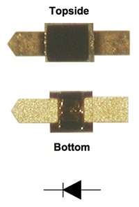
Figure 8: M/A-COM’s MA4AGBLP912 PIN diode uses AlGaAs materials; its core package is a few tenths of a millimeter on either side. (Source: M/A-COM Technology Solutions Inc.)
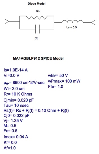
Figure 9: Vendors provide detailed models for PIN diodes such as this Spice model of the MA4AGBLP912 PIN diode; the models are needed for comprehensive circuit simulation. (Source: M/A-COM Technology Solutions Inc.)
The SMP1345 series of plastic packaged, surface-mount PIN diodes from Skyworks Solutions is designed for high-volume, low-noise-block (LNB), wireless local area network (WLAN), and switch applications from 10 MHz to 6 GHz. Devices in the family feature very low capacitance and low resistance. Key performance parameters of insertion loss (Figure 10) and isolation loss (Figure 11), show the former varies by about ±0.2 dB while the latter varies within a 35 dB range from 0 to 6 GHz.
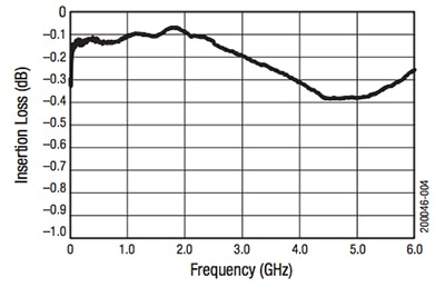
Figure 10: Skyworks Solutions' SMP1345 PIN diodes have insertion loss that is fairly flat to 6 GHz. (Source: Skyworks Solutions, Inc.)
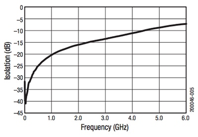
Figure 11: The isolation performance of the SMP1345 spans about four decades (in dB), which is typical of PIN diodes. (Source: Skyworks Solutions, Inc.)
The Broadcom ASML-5829 is specifically designed for low-power limiter applications. It is used to prevent damage to the receiver from large input signals, while allowing the receiver to function normally in the absence of a large signal. This device combines a PIN diode and a Schottky diode to form a low-power limiter. The PIN diode is at the input to protect the Schottky diode from high RF power levels (Figure 12). As a result, the Schottky-enhanced limiter will have a lower limiting threshold compared to the more conventional self-biased PIN-only limiter. Like many RF component data sheets, it includes S parameters for more comprehensive RF characterization and analysis (Figure 13).
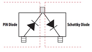
Figure 12: The Broadcom ASML-5829 combines two components often used alongside each other – the PIN diode and a Schottky diode – to implement a front-end limiter in less space and with fully characterized performance of the pairing. (Source: Broadcom Limited)

Figure 13: The ASML-5829 data sheet includes S11 and S12 parameters versus frequency enabling detailed analysis of its RF performance, here at input power levels of 0 dBm (left) and much lower -30 dBm (right). (Source: Broadcom Limited)
Conclusion
The ability to switch and route RF signals is a common requirement in wireless systems. While electromechanical switches were the dominant component used to do this many years ago, they have been superseded by solid-state solutions based on PIN diodes, FET switches, or a combination of components.
The PIN diode is an apparently "simple" passive device used in a variety of switching designs due to its speed and isolation potential. However, because it merges both the RF signal path and the DC bias to the same connection point, it requires careful understanding and consideration when assessing whether to use series, shunt, or combined approaches to build the complete switch. The availability of detailed models also enables highly accurate representations of the PIN diode and its use in the final circuit design.
Related Articles
- RF Switches Simplify Multi-Antenna Systems
- RF Switches Add Flexibility
- Semiconductor RF Switches: Small but High-Performing Circuit Components

免责声明:各个作者和/或论坛参与者在本网站发表的观点、看法和意见不代表 DigiKey 的观点、看法和意见,也不代表 DigiKey 官方政策。


