Semiconductor RF Switches: Small but High-Performing Circuit Components
投稿人:电子产品
2015-01-08
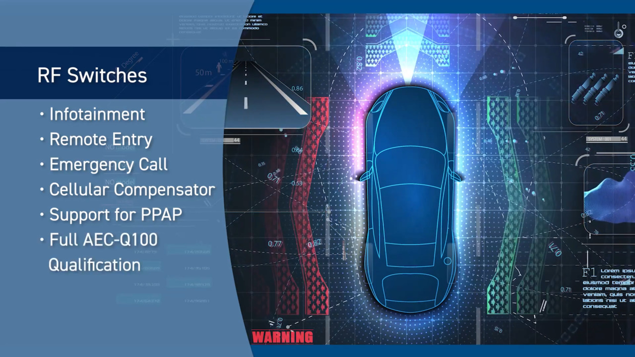
RF switches are used to select a desired signal from among multiple available sources, or to route a signal to a desired channel, in applications such as diversity antenna systems, radar, and test and measurement setups. The switches (sometimes called relays) can be built using electromechanical (EM) designs similar to a non-RF switch, but these have now been supplanted by switch ICs, except in higher-power applications where ICs are inadequate, as well as some very specialized situations or where the switch needs many poles (contacts).
There are also RF switches based on MEMS technology which replicate the electromechanical design but use IC fabrication techniques. This article focuses on IC-based solid-state switches, which begin with a SPDT (single pole/double throw) arrangement (Figure 1), and are usually built with FETs and PIN diodes as their core switching element.

Figure 1: An SPDT RF switch is conceptually simple, with a control signal directing the switch to route the input to either one of two possible outputs. (Courtesy of Skyworks Solutions)
These are many parameters which define RF switch performance, and most must be characterized versus supply voltage, temperature, frequency, power level, and other factors. Some are especially critical in a given application, while others may not be as vital. Note that most RF switches are designed for 50 Ω operation, but some are designed for the 75 Ω standard of cable TV. Given the high frequencies at which these switches operate, many vendors now offer S-parameters and Smith charts as parts for their data sheet specifications (for background see the TechZone article “The Smith Chart: An ‘Ancient’ Graphical Tool Still Vital in RF Design”), to assist engineers in determining overall signal-path performance, matching component impedances for minimal loss, and modeling-system performance.
The first parameter which engineers must check is the frequency range coverage of the switch. For example, a switch’s performance may be fully specified from 1 to 5 GHz, or 3 to 10 GHz, or just over a limited band such as the 2.4 GHz Wi-Fi band (although the switch will work to a lesser, not-guaranteed extent outside the range). Due to the underlying semiconductor physics, RF switches based on PIN diodes tend to have reduced performance at lower frequencies, while FET-based devices can operate down to very-low frequencies and even DC.
Power handling is the next critical factor. However, it is not just how much power the switch can handle before it fails, but how well it performs at different power levels. Today’s complex modulation schemes and high average-to-maximum signal power ratios mean that the switch must offer sufficient performance in linearity, adjacent channel leakage ratio (ACLR), distortion, third-order intermodulation product (IP3), and in-band error vector magnitude (EVM) at the power levels of interest.
Switching speed, which is not related to frequency range, is also important in some applications. While the definition varies among vendors, the most common definition of turn-on time is the time for the switch RF output to reach 90 percent of its final value after the change in switch “position” is initiated; turn-off time is the time to decrease to 10 percent of the final value. IC switches have turn-on/off times on the order of microseconds and even nanoseconds (compare to EM switches, which are in the millisecond range). Closely related to switching speeds, and more important in many applications, is the settling time, when the RF output settles to within 0.1 dB or even 0.05 dB of the final value, because the circuitry cannot act on a signal until it has reached very close to its final, correct valve in many applications.
Insertion loss defines the attenuation in the signal path. All IC switches induce some loss in the signal they route due to on-channel resistance, the addition of their on-resistance to the load impedance and associated signal reflection, and leakage through internal capacitance. Insertion loss is typically between 0.5 and 2 dB, and vendors can tailor the internal resistance and capacitance to minimize the loss within the specified operating frequency band, at the cost of reduced insertion loss outside that band.
The isolation specification defines the transmission of the RF signal to the disconnected (or disengaged) throws of the switch. Once again, switch designers can devise topologies which leverage device physics and which yield trade-offs in isolation at different frequencies. Thus, a wideband switch may have isolation of 80 or even 90 dB at lower frequencies, but only 30 to 40 dB at higher frequencies.
Video feedthrough characterizes voltage transients which appear at the switch outputs when the switch changes signal path, even if there is no signal at that time. It is important in design of high-gain amplifiers with AGC (automatic gain control), which are intended to intentionally decrease their gain in response to increases in signal level.
Drive and power consumption indicate what kind and how much electronic signal is needed to manage the switch control line, and how much power the switch itself — as an active device, unlike a DC switch — consumes even when it is not changing its routing path. (Note that EM switches have relatively high power needs when switching, but zero dissipation once switched, as they are passive devices.)
All switches have reliability issues. As devices with no moving parts, IC switches can operate “indefinitely” (hundreds of millions of cycles) if used within their ratings, whereas an EM switch may be specified for only several million cycles. Elevated temperate and thermal cycles, however, can decrease the life of the IC switch, and the switch can be damaged by excess applied power or ESD events.
Finally, there is switch termination configuration. RF switches are designed to be either reflective open or reflective short (sometimes called absorptive) devices. A reflective-open switch does not have a shunt path to the system ground on the open connection, and so minimizes the load on the unused port. In contrast, the reflective-short switch configuration has a 50 Ω termination path (shunt) to ground so there is no reflection on the signal line, and thus there is a low VSWR (vertical- standing wave ratio) regardless of switch state. Many switches are available in both formats but with otherwise nearly identical specifications.
Diverse ICs serve different needs
The Hittite Microwave Corp. (now part of Analog Devices, Inc.) HCM545 is a basic GaAs SPDT switch, (Figure 2), specified for DC through 3 GHz operation, targeted at cellular infrastructure, wireless LANs, automotive designs, and test equipment. It features 0.25 dB typical loss and input IP3 of +65 dBm, and is designed with reflective shorts on its ports when “off”. It is controlled by a CMOS/TTL signal (0/+3 V to 0/+8 V) and is housed in a small, 6-lead SOT26 plastic package.

Figure 2: The Hittite HCM545 uses a basic 74C-series CMOS driver to operate the signal-path control pin.
For higher-frequency coverage but without DC performance, the reflective short SKY13350-385LF GaAs SPDT switch from Skywork Solutions covers 0.01 to 6.0 GHz, with typical insertion loss of 0.35 dB and 25 dB typical isolation, both measured 3 GHz. It can handle up to 32 dBm power with a 10/90 percent switching speed of 45 ns. As with nearly all RF components, performance is a function of supply voltage; Figure 3 shows the EVM versus output power for a range of supply voltages, in the IEEE 802.11a 5.2 to 5.8 GHz band.

Figure 3: Nearly all active RF components are sensitive to supply voltage, temperature, and power level; here is the variation of EVM versus both supply voltage and power level for the SKY13350-385LF from Skyworks Solutions.
For designs which go into much higher frequencies, the M/A-Com MASW-002103-1363 SPDT switch is specified from 50 MHz to 20 GHz, and is usable up to 26 GHz; power handling capability is 38 dBm. Insertion loss, (Figure 4), is approximately 0.4 dB at the low end of the range, increasing to 1.0 dB at 20 GHz and 1.6 dB at 25 GHz.

Figure 4: The insertion loss of a switch increases with increase on frequency; here, the M/A-Com MASW-002103-1363 SPDT switch loss is shown from just above DC to 26 GHz.
While most RF switches use GaAs or CMOS technology, Peregrine Semiconductor uses a proprietary UltraCMOS process (a patented variation of silicon-on-insulator (SOI) technology on a sapphire substrate) offering what they claim is the performance of GaAs with the economy and integration of conventional CMOS. Their PE42520MLBA-Z absorptive RF switch is designed for test/ATE and wireless applications. It features a frequency range of 9 kHz through 13 GHz with a power-handling rating of 36 dBm continuous wave (CW) and 38 dBm instantaneous power @ 8 GHz in 50 Ω. Insertion loss is 0.8, 0.9, and 2.0 dB at 3, 10, and 13 GHz, respectively, while isolation is 45, 31, and 18 dB at those same frequency points. As with all RF switches, insertion loss is also a function of temperature (Figure 5).

Figure 5: Insertion loss, like most other switch parameters, is also a function of temperature; for the Peregrine Semiconductor PE42520MLBA-Z SPDT switch, it increases about 0.5 dB from -40⁰C to +85⁰C.
Summary
A complicated signal-chain front-end may easily have a double-digit number of switches between antenna and processor to support multiple bands, functions, and application requirements. While an RF switch is functionally similar to a DC or power switch, the internal design and specifications of interest are very different. Every RF switch balances a wide variety of performance characteristics and trade-offs (as well as cost issues), beginning with frequency range of operation, and then continuing to insertion loss, power rating, isolation, and switching speed, among many others. Designers must look carefully at typical specifications as well as maximum/minimum values, and also examine unavoidable performance variations versus supply, temperature, and power levels.
For more information on the parts discussed in this article, use the links provided to access product information page on the DigiKey website.
免责声明:各个作者和/或论坛参与者在本网站发表的观点、看法和意见不代表 DigiKey 的观点、看法和意见,也不代表 DigiKey 官方政策。