Getting Started With NFC
投稿人:DigiKey 欧洲编辑
2013-06-13
Near-Field Communication (NFC) is an evolution of radio frequency identification (RFID) tag technology that allows objects to respond to the tap of a mobile device. Although the tags are being used for making payments from a wireless bank card or a mobile phone, there are many more applications. NFC takes the identification and low cost capabilities of RFID and extends them with processing and authentication within the NFC tag. This transforms the already dynamic mobile user experience in a way that enables the "Internet of Things". Tags in "smart posters" or location based check-in signs, games or media content on a friends' tablet, and ticketing or payment terminal contactless readers can now interact with your mobile device in a secure yet simple way. NFC technology is even being used in secure access systems to replace locks and to provide information on the label of a wine bottle.
There are a number of NFC standards available, operating in the 13.56 MHz unlicensed band, but the new generation of tag readers supports a wide range of bands to allow designers to implement systems that read a wide range of different tags. This interoperability creates the broad ecosystem that is essential to increase the volume usage of the tags and so bring the costs down to the point where NFC can be ubiquitous.
NFC standardizes a super set of technology from three vendors, including NXP, and provides links up to 424 kbit/s for low traffic applications such as setting up links for faster links such as Bluetooth or transferring a web address that can be downloaded via a Wi-Fi or 3G network.
Four types of tag have been defined, based on ISO 14443. Types A and B are defined for contactless smartcards. A flexible reader should be able to handle each type. The FeliCa format from Sony conforms to the passive communication mode standard, ISO 18092.
| Standard | Capability | Memory | Data rate | Notes | |
| Type 1 | ISO14443A | Read Rewrite |
96 bytes, expandable to 2 kbytes | 106 kbit/s | Simple, cost effective and ideal for many NFC applications |
| Type 2 | ISO14443A | Read Rewrite Read only |
48 bytes, expandable to 2 Kbytes | 106 kbit/s | |
| Type 3 | ISO 18092 FeliCa |
Read Rewrite |
2 Kbytes | 212 kbit/s | Higher cost, more complex applications |
| Type 4 | ISO14443A and B | Read Rewrite Read only Configured at manufacture |
32 kbytes | Between 106 kbit/s and 424 kbit/s |
The technology falls into three categories:
- Service initiation such as setting up a link to a smart printer, poster or photo frame
- Peer-to-peer links
- Payment and ticketing
Evaluation system
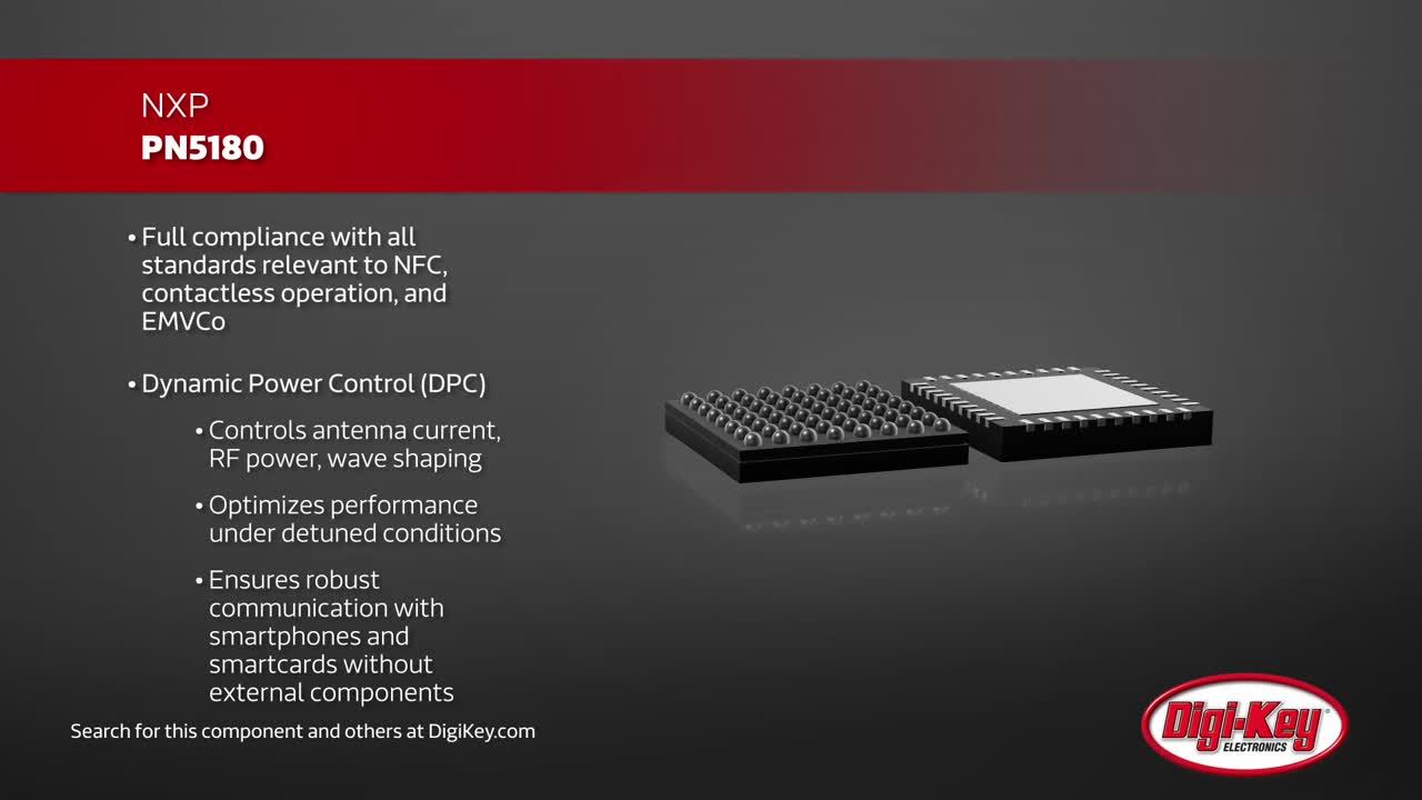
The NXP Semiconductor controller IC PN532 used in the evaluation kit is a highly integrated transmission module including a microcontroller that reduces the processing power from the host controller. The PN532 offers proximity connectivity targeting 13.56 MHz reader/writer applications for point of sales (POS) terminals and handheld devices and is also capable of acting as a smart card when combined with a secure element.
The reader/writer architecture (Figure 1a) allows easy pairing of Bluetooth-, Wi-Fi-, or Wireless USB-enabled devices, and reading and writing of NFC Forum tags such as MIFARE, MIFARE Ultralight, DESFire, Felica and Topaz. Used in the peer-to-peer mode, the tags can exchange data such as business cards or small pictures.
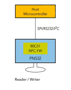
The POS terminal design (Figure 1b) requires two additional RF transistors and a few passives to handle EMV banking transactions such as PayPass™ and VisaWave, and opens up the possibility of connecting to a SAM (Secure Access Module) through the smart card controller.
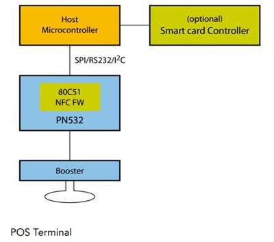
The card emulation functionality (Figure 1c) is compatible with ISO14443 A when connected to a secure controller, and provides an operating distance of up to 10 cm. This allows the device to be used as a POS Terminal and perform secure transactions when connected to an NXP recommended RF amplifier. This makes it possible to emulate a MIFARE card to access public transport, stadiums, or buildings, or to a store loyalty program or pre-paid wallet. The emulation mode can also be used as an EMV payment card.
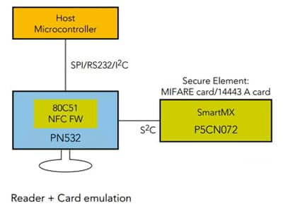
Inside the PN532 is an optimized 80C51 core processor with embedded firmware in ROM to relieve the host controller from real time processing tasks, and it is supported by multiple interfaces (UART, SPI and I²C) to link to external peripherals. The chip also includes an integrated MIFARE cipher crypto engine for security.
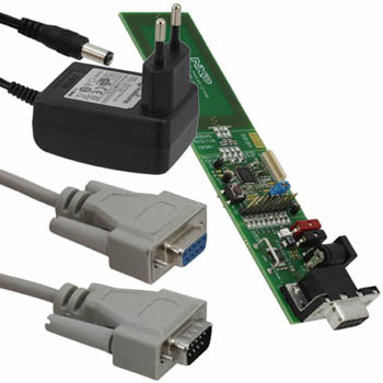
Footprint is vital for such system designs, and the PN532 comes in a QFN40 package measuring 6 x 6 x 1 mm as seen in the evaluation kit (Figure 2).
Adding custom PFC protocols
The TRF7970A from Texas Instruments (Figure 3) is an integrated analog front end and data-framing device for a 13.56 MHz NFC communication system. Built-in programming options make it suitable for a wide range of applications for proximity and vicinity identification systems, supporting both ISO14443 and ISO15693, as well as custom protocols.
It can perform in one of three modes: RFID/NFC Reader, NFC Peer, or in Card Emulation mode. Built-in user-configurable programming options make it suitable for a wide range of applications. The TRF7970A is configured by selecting the desired protocol in the control registers, and direct access to all control registers allows fine-tuning of various reader parameters, as needed.
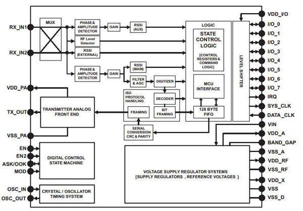
The built-in data framing supports ISO15693, ISO14443A, ISO14443B, and FeliCa and includes data rates up to 848 kbps for ISO14443 with all framing and synchronization tasks onboard (in default mode). The TRF7970A also supports NFC Tag Type 1, 2, 3 and 4 operations. This architecture enables the designer to build a complete cost-effective yet high performance multi-protocol 13.56 MHz RFID/NFC system together with a low-cost microcontroller (for example the MSP430).
Other standards and even custom protocols can be implemented by using two of the Direct Modes that the device offers. These Direct Modes (0 and 1) allow the user to fully control the analog front end (AFE) and also gain access to the raw subcarrier data or the unframed but already ISO formatted data and the associated extracted clock signal.
The receiver system has dual input receiver architecture. The received input bandwidth can be selected to cover a broad range of input subcarrier signal options and the received signal strength from transponders, ambient sources, or internal levels is available through the RSSI register for use by applications.
The receiver output is selectable among a digitized subcarrier signal and any of the integrated subcarrier decoders which deliver the data bit stream and the data clock as outputs.
The TRF7970A also includes a receiver framing engine to handle the CRC and parity checks, remove the EOF and SOF settings, and organize the data in bytes for ISO14443-A/B, ISO15693, and FeliCa protocols. This framed data is then accessible to the microcontroller through a 128-byte FIFO register, although the encoders and decoders can be bypassed so that the MCU can process the data in real time, if desired.
The transmitter has selectable output-power levels of 100 mW (+20 dBm) or 200 mW (+23 dBm) equivalent into a 50 Ω load when using a 5 V supply and supports OOK and ASK modulation with selectable modulation depth.
The TRF7970A also includes a data transmission engine that comprises low-level encoding for ISO15693, ISO14443A/B and FeliCa. Included with the transmit data coding is the automatic generation of Start Of Frame (SOF), End Of Frame (EOF), Cyclic Redundancy Check (CRC), or parity bits.
Several integrated voltage regulators ensure a proper power-supply noise rejection for the complete reader system. The built-in programmable auxiliary voltage regulator VDD_X (pin 32) is able to deliver up to 20 mA to supply a microcontroller and additional external circuits within the reader system.
The desired bit rate is set by selecting the option bits in control registers. The transmitting system consists of a programmable RF level detector, which is used for the initial (or response) RF collision avoidance. The RF collision avoidance sequence is started by sending a direct command. If successful, the NFC initiator can send the data or commands that the MCU has loaded in the FIFO register. The coding of this data is done by hardware coders in either ISO14443A/B format or in FeliCa format. The coders also provide CRC and parity bits (if required) and automatically add preambles, SOF, EOF, and synchronization bytes as defined by selected protocol.
The receiver provides the integrated decoders for both active and passive ISO14443A/B and FeliCa tags with all the framing including CRC and parity check and removal of SOF, EOF, and synchronization bytes as specified by the selected protocol.
Activating the target tag
The activation of NFC target is done when a sufficient RF field level is detected on the antenna. The level needed for wake-up is selectable and is stored in a non-volatile register.
When the activation occurs, the system automatically powers up and waits for the first command to be received. Based on this command, the system knows if it should operate as a passive or active target and at what bitrate.
To operate as an NFC target or tag, the MCU must load a value different than zero (0) in the Target Detection Level register to enable the RF measurement system. This can operate also during complete power down, consumes only 3.5 µA, and constantly monitors the RF signal on the antenna input. When the RF level on the antenna input exceeds the level defined in the Target Detection Level register, the chip is automatically activated (and the internal EN line is forced high). When the voltage supply system and the oscillator are started and are stable, osc_ok goes high (B6 of RSSI Level and Oscillator Status register) and IRQ is set.
When the first command from the INITIATOR is received, another IRQ signal is sent with B6 set in the IRQ register. The MCU must set EN to high in the time between the two IRQs because the internal power-up ends after the second IRQ.
The type and coding of the first initiator (or reader in the case of a tag emulator) command defines the communication protocol type that the target must use, so the communication protocol type has to be available in the NFC Target Protocol register immediately after receiving the first command.
Based on the first command from the INITIATOR, the commands are set for the different types and data rates of tags:
- If the first command is a POLLING request, the system becomes the TARGET in passive communication using 212 kbit/s, or 424 kbit/s for FeliCa tags.
- If the first command is ATR_REQ, the system operates as an active TARGET using the same communication speed and bit coding as used by the INITIATOR. Again, all of the replies are handled by the MCU.
- If the first command is coded as ISO14443B and the Tag emulation bit is set in the ISO Control register, the system enters ISO14443B emulation mode. The anti-collision must be handled by the MCU, and the chip provides all physical level coding, decoding, and framing for this protocol.
Active target
If the first command received by the RF interface defines the system as an active target, then the receiver selects the appropriate data decoders (ISO14443A\B reader or FeliCa) and framing option. Only the raw (decoded) data is forwarded to the MCU through the FIFO, while the SOF, EOF, preamble, sync bytes, CRC, and parity bytes are checked by the framer and discarded.
The transmitting system uses the programmable RF level detector for collision avoidance, and the sequence is started by sending a direct command. If successful, the NFC initiator can send the data that the MCU has loaded in the FIFO register. The coding of this data is done by hardware coders, either in ISO14443A format at 106 kbit/s or in FeliCa format at 212 kbit/s or 424 kbit/s. The coders also provide CRC and parity bits (if required) and automatically add preambles, SOF, EOF, and synchronization bytes as defined by selected protocol.
Passive target
If the first command received by the RF interface defines the system as a passive target, then the receiver selects the appropriate data decoders (ISO14443A\B reader or FeliCa) and framing option. Again, only the raw (decoded) data is forwarded to the MCU through the FIFO; SOF, EOF, preamble, sync bytes, CRC, and parity bytes are checked by the framer and discarded. The receiver works the same as in the case of an active target.
For a passive target at 106 kbit/s, an internal single device detection (SDD) state machine is available and can perform the SDD (using the same anti-collision algorithms used in RFID tags) as defined in ISO14443A\B. This relieves the MCU of the demanding task of handling the 'broken bytes'. For synchronization with the Initiator, a 13.56 MHz clock extractor with a glitch-free switch unit between the internal and external clock is integrated. The clock extractor can be disabled by the application.
The transmit system in passive target mode is different as there is no RF collision avoidance sequence, and encoders are used to code the data for an ISO14443A\B tag at 106 kbit/s or FeliCa at 212 kbit/s. The coding system adds all of the SOF, EOF, CRC, parity bits, and synchronization bytes required by protocol. On the physical level, the modulation of the initiator's RF field is done by changing the termination impedance of the antenna between 4 Ω and open.
Card emulation
The chip can enter the card emulation mode by setting option bits for ISO14443A/B with a 106 kbit/s data rate. For ISO14443A, the anti-collision algorithm can be performed using an internal state machine, which relieves the MCU of any real-time tasks. The unique ID required for anti-collision is provided by the MCU after wake-up of the system.
Conclusion
While there is a significant number of different standards and different modes of operation for NFC systems, the flexibility and programmability of current hardware allows these to be easily recognized and implemented. They rely on the initialization to provide the key information for which tags are involved in the transaction, but optimized controller code and access to the core registers provide the relevant data. State machines are used to put the reader into the appropriate state for the data transfer, and the evaluation and development hardware allows higher-level applications that use these transfers to be tested out on the hardware.

免责声明:各个作者和/或论坛参与者在本网站发表的观点、看法和意见不代表 DigiKey 的观点、看法和意见,也不代表 DigiKey 官方政策。
