Extending Battery Life in Wearable Designs
投稿人:电子产品
2015-05-19
The wearables market is booming. Statistics aggregator web portal Statista, notes that the global market will be worth over $7 billion this year and $12.6 billion by 2018.
Although the potential rewards are high, this is not an easy market to enter. Designing smart watches or fitness bracelets is tough; consumers expect lots of functionality, smartphone connectivity, compact form-factor, light weight, and long battery life. The introduction of highly integrated, ultra-low-power microprocessors and wireless chips has eased the design process, but squeezing out all of the battery’s power remains key to a wearable product’s success.
This article takes a look at how silicon vendors help wearables designers extend battery life by offering power-frugal displays, microcontrollers (MCU), silicon radios, and power-management chips designed specifically for ultra-low-power applications.
Convergence of technology
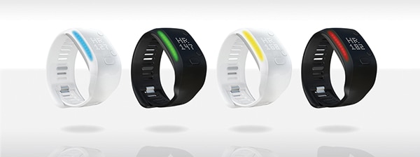
Wearables have sprung to the fore because of the convergence of three key technologies1. Ultra-low-power chips that can run from watch batteries allow companies to offer compact products which, thanks to smartphone-compatible wireless technology such as Bluetooth Smart (also known as Bluetooth low energy), communicate seamlessly with smartphones and tablets. A range of inexpensive apps presents the information gleaned from the wearable in a user-friendly format indicating, for example, how long the user needs to exercise to lose weight. A recent leading-edge wearable is adidas’ Fit Smart wristband tracker which incorporates Bluetooth Smart technology from Nordic Semiconductor (Figure 1).

Figure 1: adidas’ Fit Smart is typical of the latest generation of wearable products. (Courtesy of adidas/Nordic Semiconductor)
Products such as the Fit Smart combine multiple facets of engineering including advanced electronics such as 32-bit MCUs, 2.4 GHz silicon radios, analog-to-digital converters (ADC), and display drivers. In addition, a wearable could incorporate several sensors measuring atmospheric pressure, humidity, temperature, and acceleration. The capability of the MCU significantly affects the performance of the device and determines its market appeal; the MCU also often integrates other elements of the wearable’s electronics such as the Bluetooth Smart radio and the ADC. However, that’s not the whole story.
Wearables must be unobtrusive; that places constraints on size and weight and, in turn, on the capacity of the power source. Some wearables, such as smart watches with powerful computation capabilities and GPS, will be designed to draw on the resources of rechargeable Li-ion batteries and consumers accept the requirement to top up the cell occasionally. However, if the frequency of recharges can be reduced the product may gain an edge over a competitor.
Other wearables, such as fitness bracelets, are expected to run for months without cell changes. Technologies such as ARM-based low-power embedded processors or optimized microcontrollers such as Texas Instruments’ (TI) MSP430 and “ultra-low-power” wireless connectivity such as Bluetooth Smart, RF4CE, or ZigBee help engineers design devices that can run tiny batteries such as CR2032 coin cells. For this type of battery to last several months, average current draw must be limited to just a few milliamps. That restricts a product to perhaps a few tens of milliamps when operating normally and tens of microamps or even a few hundred nanoamps when in sleep mode (see the TechZone article “Tiny Voltage Regulators Meet Wearable Electronics Space Constraint.”).
Designing for low power
The display (if one is fitted), MCU, and silicon radio are responsible for the majority of the power draw in a wearable device. Manufacturers attempt to limit the display-power consumption by using technologies such as organic LED (OLED) displays. OLEDs consume less power than conventional LEDs because they do not need any backlighting. The technology also lends itself to thinner and lighter displays (see the TechZone article “OLEDs Move Closer to Mainstream Lighting”). To save even more power, these displays present minimal information because the consumer is typically able to retrieve lots of statistics from an associate app on their smartphone, and the displays switch to power-saving modes quickly when not being accessed.
The MCU in a wearable needs to deal with some heavy computational work while minimizing power consumption. Fortunately, silicon vendors have lots of experience in optimizing this trade-off in mobile devices such as cellphones and mp3 players. Techniques such as high-clocking rates to get the work done quickly and allow the MCU to return rapidly to a low-power sleep state minimize static power losses and extend battery life (see the TechZone article “Design Techniques for Extending Li-Ion Battery Life”).
Also helping the design engineer to make the most of his or her power budget are wireless connectivity technologies such as Bluetooth Smart and ZigBee. These are specifically designed to save power by transmitting data in rapid bursts so that they can return to low-power sleep modes quickly and by limiting transmission range to perhaps 10 meters. Bluetooth Smart, for example, differs from conventional Bluetooth wireless technology by employing an asynchronous RF protocol that, unlike its bigger brother, does not have to remain constantly “on air” to maintain pairing – saving precious battery power.
Design engineers should also be aware that the type of sensors often used in wearable products can exhibit quite high leakage currents even when “shut down,” so provisions should be made to actively disconnect such devices from the supply rails with a hard switch rather than merely allowing them to power down.
Power management
Despite the array of low-power consumption chips available, developing a wearable product with decent battery life is far from trivial. In fact, power management can make or break a product. Successful wearables often combine both popular voltage regulator technologies, teaming the high efficiency of a switching voltage regulator with the “clean” power of a low drop-out linear regulator (LDO).
A switching regulator is efficient over wide voltage- and load-range, but the voltage- and current-ripples at the output can play havoc with sensitive mixed-signal chips, particularly silicon radios. By passing the switching regulator’s output through an LDO, ripples can be smoothed. Because the LDO’s efficiency is proportional to output voltage divided by input voltage, the design engineer should ensure the switching regulator’s output (i.e., the LDO’s input) is close to the LDO’s output, extending battery life. The lower the drop-out voltage of the LDO, the closer these voltages can be matched.
Many manufacturers offer power modules that integrate switching regulators and one or more LDOs into a single chip. Examples include TI’s TPS61130––which integrates a 500 kHz switching regulator with an LDO in a module which produces two 2.5 to 5.5 V (300 and 320 mA) outputs––and Maxim’s MAX 1765, which again offers two outputs, 2.5-5.5 V (800 mA) and 2.85-to-adjustable (500 mA). For more information see the TechZone article “Power Modules Combine Efficiency with Low-Noise Output.”
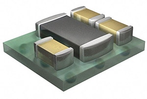
Products such as TI’s TPS82740A take things even further; the module is specifically designed to look after the power requirements of wearables such as smart watches. The company offers the device in a “MicroSIP” (System-in-Package) that includes the switching regulator, inductor, and input/output capacitors in a package with a volume of only 6.7 mm². No external components are needed, making the TPS82740A a good choice for space-constrained wearables (Figure 2).

Figure 2: TI’s MicroSIP-packaged switching regulator measures just 6.7 mm² and requires no external components.
Although the TPS82740A does not combine a switching regulator with an LDO, instead just employing the services of a step-down (“buck”) switching regulator, TI claims that the output is virtually ripple-free and does not upset sensitive circuits. One clever trick that the module plays is to revert to 100 percent duty cycle when the input voltage is close to the output voltage (effectively mimicking an LDO). The module operates from an input-voltage supply range of 2.2-5.5 V with a maximum output current of 200 mA.
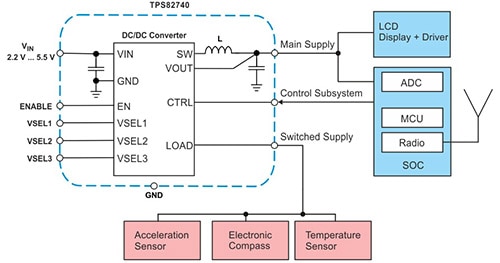
Figure 3 shows a schematic of a wearable product employing the TPS82740A. A common voltage is used for the MCU, radio, and sensors. The MCU is connected directly to the output of the switching regulator and thus is always powered. The sensors are connected to the output of an integrated load switch, which is closed only when the user requests data, saving power.

Figure 3: Schematic of power supply in a wearables application. Sensors are switched off when not in use to limit leakage currents and save power. (Courtesy of Texas Instruments)
One drawback of switching regulators is that efficiency tails off at low loads. This can compromise battery life if unchecked because wearable products typically spend long periods in low power “sleep” or “standby” modes with little user interaction. Chip vendors have addressed this drawback of switching regulators at low loads by either varying the switching frequency, skipping pulses, or even suspending operation altogether until that output voltage drops below a certain threshold. All these techniques are designed to reduce switching losses which become much more significant as loads decrease (see the TechZone article “Using PFM to Improve Switching DC/DC Regulator Efficiency at Low Loads”).
TI employs a proprietary technique the company calls DCS-Control (“Direct Control with Seamless Transition into Power Save Mode”) in the TPS82740A. At high load currents, the switching regulator operates in quasi-fixed frequency pulse width modulated (PWM) mode. The maximum switching frequency is 1.7 MHz. As the load current decreases, the module enters a power-save mode by varying the switching frequency linearly. At very light loads, the module generates a single-switching pulse to ramp up the inductor current and recharge the output capacitor, returning to a 360 nA quiescent current-consumption mode until the output voltage drops below a set threshold.
While designing wearables is tough, manufacturers offer purpose-designed low-power chips and a wealth of engineering advice to make life a little easier for engineers. The good news it that consumers have taken to wearables in a big way; consequently lucrative awards await companies that follow in Garmin, adidas, and Fitbit’s footsteps with efficient, useful monitoring products allied to clever smartphone apps.
For more information about the parts discussed in this article, use the links provided to access product pages on the DigiKey website.
References:
- “Technology convergence powers wearables boom,” ULP Wireless Q, Nordic Semiconductor, Autumn 2014.
免责声明:各个作者和/或论坛参与者在本网站发表的观点、看法和意见不代表 DigiKey 的观点、看法和意见,也不代表 DigiKey 官方政策。


