Enhancing the Wireless Interface
投稿人:DigiKey 欧洲编辑
2012-02-16
Wireless is rapidly becoming the technology of choice for the human interface. Being able to wave a remote control unit to make changes to a system is being more frequently demanded by users. This article looks at the range of RF technologies available for wireless remote controls, from Zigbee RF4CE to keyless entry systems.
Remote controls are changing. No longer are they simple infrared keypads, but increasingly important elements of overall industrial system design. Significantly longer distances and no need for line-of-sight are contributing to the popularity of radio for remote controls.
All this is largely being driven by improvements in wireless technology, particularly battery life, but also the processing power to handle new protocols and the security that is needed when the remote control moves over to radio.
New protocols such as the Zigbee variant RF4CE allow mainstream industrial and home automation wireless networking technology to be used for remote control, bringing the advantages of volume production and leading edge silicon process technology to the segment.
However, there are more opportunities for highly efficient low data rate RF devices to provide the low power and long battery life that is vital for remote control applications. The lower frequencies allow longer range or the same range with lower power and so enhance battery life.
As these devices are simpler than the 2.4 GHz Zigbee designs, they lend themselves to higher levels of integration, reducing power by reducing external components and the power penalty of moving off chip, and reducing costs with higher integration and volumes. This in turn helps drive more remote control into applications such as keyless entry systems to replace the everyday lock.
Silicon Labs has developed system-on-chip (SoC) transmitters, such as the Si4010 single-chip remote control integrated circuit (IC), that greatly simplify the process of designing a remote control and reduce system bill of materials (BOM) cost by eliminating the need for numerous discrete components.
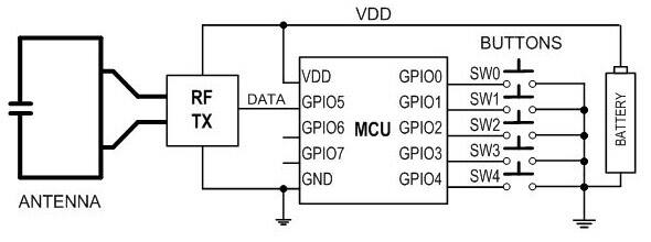
Figure 1: Simplified block diagram of an RF remote control.
All RF remote controls share common features as shown in the simplified block diagram in Figure 1. The basic components of an RF remote control are buttons for the user to input a command, a microcontroller unit (MCU) to process the user commands into digital messages, an RF transmitter (RF TX) to modulate and transmit the message, an antenna, and a battery to provide power to the remote control. The common challenges manufacturers face in designing RF remote controls are to provide consistent maximum transmission range, ensure long battery life, and maintain low system costs.
Maximizing transmission range involves transmitting as much power as possible while providing a receiver with excellent sensitivity.
From the remote control side, the design goal is to set the RF output power to the government limit, allowing for manufacturing tolerances and the impact of the user on the output power. This can reduce the effective radiated power (ERP) of a remote control and result in output power 6 dB below the limit and halving the range.
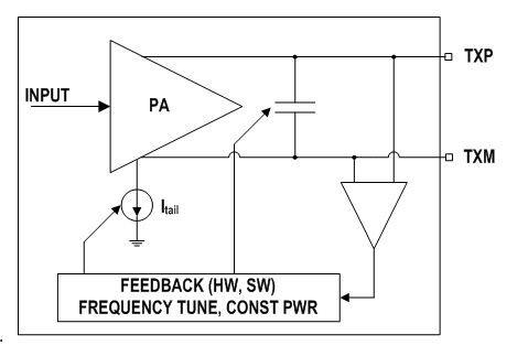
Figure 2: Si4010 antenna tuning block diagram.
Silicon Labs Si4010 transmitter is the industry’s first single-chip remote control IC, requiring only one external bypass capacitor, a printed circuit board (PCB), battery, and an external casing with push buttons to form a complete remote control. It includes a patented antenna tuning circuit that automatically fine-tunes the antenna for optimum transmit power on every button press to compensate for those real world variations.
This is done by adjusting an on-chip variable capacitor to resonate with the inductance of the antenna to maximize the transmit power of the remote control. It also has the benefit of reducing design cost by relaxing the manufacturing tolerances in the PCB antenna.
An additional feedback loop is incorporated into the power amplifier (PA) to maintain constant output power by monitoring the voltage at the output of the PA and adjusting the PA’s current drive to compensate for changes in the antenna impedance. This feedback loop works to maintain constant output power in spite of temperature variations and the “hand effect,” which, as stated above, changes the antenna impedance when a person’s hand is covering the remote control. The net result of antenna tuning is to provide consistently reliable and optimal performance on every button press while reducing the cost and design complexity of the RF matching requirements.
The static power when the remote is waiting for an input is the key figure for such designs, and the Si4010 consumes less than 10 nA at room temperature. This is helped by having GPIO ports that wake up on touch to further minimize current consumption of the remote control and extend the battery life.
During transmission, the Si4010 consumes either 14.2 mA in on-off keying (OOK) mode or 19.8 mA in frequency-shift keying (FSK) mode while transmitting at +10 dBm output power. For a data rate of 1 kBaud and each data packet is 100 bits long and repeats three times for each button press, then we have the following results: at 50 button presses per day for five consecutive years, we use only 52 percent of the charge in a 220 mAhr CR2032 battery in OOK mode and 71 percent of the charge in FSK mode.
Freescale, for example, has developed an evaluation board, the ZSTAR3 that combines multiple digital and analog accelerometer boards with an RF ZigBee 2.4 GHz communication link to a single USB node connected to a PC.
The USB node is a key part of the ZSTAR design as it provides the dedicated software for supporting multiple nodes.
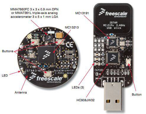
Figure 3: The Xstar3 remote control evaluation kit.
The software demonstrates the built-in intelligence of the MMA7660FC accelerometer for applications with orientation, shake, tap detection, auto-wake and auto-sleep. This links to the MC1321x 2.4 GHz low-power transceiver that is combined with an S08 microcontroller in one package. The combined transceiver and modem has 16 selectable channels to avoid interference from other 2.4 GHz sources, such as microwaves and WiFi, and a programmable output power with multiple power saving modes to get the most out of the remote’s batteries. For that reason, it operates at 2 V to 3.4 V with on-chip voltage regulators to provide the RF voltages.
Atmel also has a high performance RF-CMOS 2.4 GHz radio transceiver for IEEE 802.15.4 ZigBee RF4CE applications as well as designs in other ISM bands.
It has focused on the link budget of 104 dB from a receiver sensitivity of -101 dBm to reduce the output power and the battery life in remote controls. The output power is programmable from -17 dBm up to +3 dBm with an easy-to-use interface where the registers, frame buffer and AES encryption are accessible through a fast SPI line. This means only two microcontroller GPIO Lines are necessary with one interrupt pin from the radio transceiver. The transceiver includes a 128 byte FIFO (SRAM) for data buffering as well as an integrated Rx/Tx switch and a programmable clock output. This can be used to clock the host microcontroller or as a timer reference.
There is special hardware support for the IEEE 802.15.4-2006 standard as well as a MAC hardware accelerator.
Ember has been at the forefront of the development of Zigbee networks and its EM250 is a single-chip solution that integrates a 2.4 GHz, IEEE 802.15.4-compliant transceiver with a 16 bit XAP2b microprocessor.
The transceiver uses an efficient architecture that exceeds the dynamic range requirements imposed by the IEEE 802.15.4-2003 standard by over 15 dB. The integrated receive channel filtering allows for co-existence with other communication standards in the 2.4 GHz spectrum such as IEEE 802.11g and Bluetooth. The integrated regulator, VCO, loop filter, and power amplifier keep the external component count low.
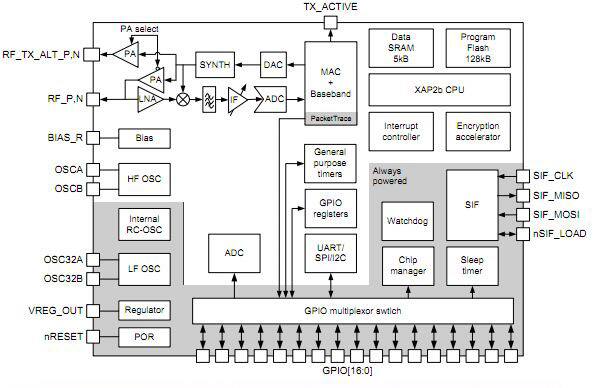
Figure 4: The Ember EM250 Zigbee transceiver.
The XAP2b microprocessor is a power-optimized core integrated in the EM250. It supports two different modes of operation—System Mode and Application Mode. The EmberZNet stack runs in System Mode with full access to all areas of the chip. Application code runs in Application Mode with limited access to the EM250 resources; this allows for the scheduling of events by the application developer while preventing modification of restricted areas of memory and registers. This architecture results in increased stability and reliability of deployed solutions.
The EM250 has 128 kB of embedded Flash memory and 5 kB of integrated RAM for data and program storage.
To maintain the strict timing requirements imposed by ZigBee and the IEEE 802.15.4-2003 standard, the EM250 integrates a number of MAC functions into the hardware. The MAC hardware handles automatic ACK transmission and reception, automatic backoff delay, and clear channel assessment for transmission, as well as automatic filtering of received packets. In addition, the EM250 allows for true MAC level debugging by integrating the Packet Trace Interface.
To support user-defined applications, a number of peripherals such as GPIO, UART, SPI, I2C, ADC, and general-purpose timers are integrated. Also, an integrated voltage regulator, power-on-reset circuitry, sleep timer, and low-power sleep modes are available. The deep sleep mode draws less than 1 μA, allowing products to achieve long battery life.
Finally, the EM250 uses the non-intrusive SIF module for powerful software debugging and programming of the XAP2b microcontroller.
Not all the options for remote controls sit with the Zigbee protocols or in the 2.4 GHz band. Analog Devices has developed a low power, highly integrated FSK/ASK/OOK transceiver designed for operation in the license-free ISM bands at 433 MHz, 868 MHz, and 915 MHz, as well as the proposed Japanese band at 950 MHz.
Low power and lower data rates are ideal for a secure remote control design, and the ADF7020 has a programmable output power of −16 dBm to +13 dBm in 0.3 dBm steps.
A Gaussian data filter option is available to allow either GFSK or G-ASK modulation, which provides a more spectrally efficient modulation to keep power consumption to a minimum. The ADF7020 can also be used to perform both MSK and GMSK modulation, where MSK is a special case of FSK with a modulation index of 0.5.
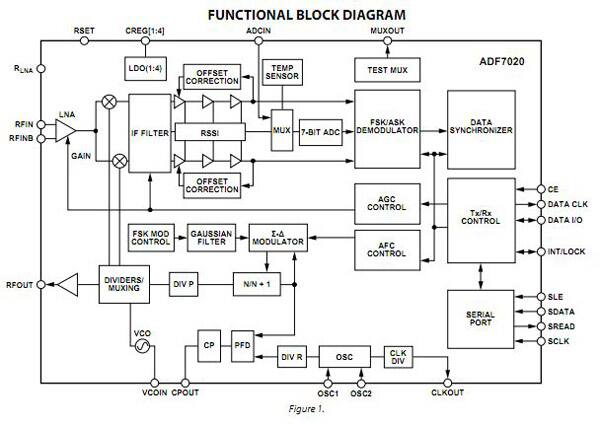
Figure 5: Analog Devices’ ADF7020 transceiver IC.
A low IF architecture is used in the receiver (200 kHz) to minimize power consumption and the external component count and to avoid interference problems at low frequencies. The receiver also features a patent-pending automatic frequency control (AFC) loop, allowing the PLL to track out the frequency error in the incoming signal.
An on-chip ADC provides read-back of an integrated temperature sensor, an external analog input, the battery voltage, or the RSSI signal, which provides savings on an ADC in some applications. There are also simpler protocols that can be used for a remote control. Maxim’s MAX7032 crystal-based, fractional-N transceiver is designed to transmit and receive ASK/OOK or FSK data in the 300 MHz to 450 MHz frequency range with data rates up to 33 kbps (Manchester encoded) or 66 kbps (NRZ encoded). It generates a typical output power of +10 dBm into a 50 Ω load, and exhibits typical sensitivities of -114 dBm for ASK data and -110 dBm for FSK data. The MAX7032 has separate transmit and receive pins and provides an internal RF switch that can be used to connect the transmit and receive pins to a common antenna.
A key point of the MAX7032 is that the transmit frequency is generated by a 16-bit, fractional-N, phase-locked loop (PLL), while the receiver’s local oscillator (LO) is generated by an integer-N PLL. This hybrid architecture eliminates the need for separate transmit and receive crystal reference oscillators because the fractional-N PLL allows the transmit frequency to be set within 2 kHz of the receive frequency. The 12 bit resolution of the fractional-N PLL allows frequency multiplication of the crystal frequency in steps of fXTAL/4096. This avoids the higher current drain requirements of a fractional-N PLL and keeps the receiver current drain as low as possible.
This also means the transmit FSK signal can be programmed for exact frequency deviations, and completely eliminates the problems associated with oscillator-pulling FSK signal generation. All the frequency-generation components are integrated on-chip, and only a crystal, a 10.7 MHz IF filter, and a few discrete components are required to implement a complete antenna/digital data solution for two-way remote keyless entry and remote controls.
The developments in CMOS have driven power consumption down to the point where highly integrated RF transceivers are viable for remote control applications. From simple protocols running in the ISM band to more complex high-level protocols such as Zigbee at 2.4 GHz, there is a wide range of options for designers to enhance the human interface with wireless technology.

免责声明:各个作者和/或论坛参与者在本网站发表的观点、看法和意见不代表 DigiKey 的观点、看法和意见,也不代表 DigiKey 官方政策。


