Digital Signal Controllers: Making the Case for ARM Cortex-M4-based Solutions
投稿人:电子产品
2012-02-15
While a number of major players in the microcontroller (MCU) space have moved to ARM-based CPU cores such as the Cortex-M3 and Cortex-M0 for general-purpose applications, the same trend is now unfolding in the digital signal controller (DSC) area in which MCUs integrate DSP-centric capabilities.
STMicroelectronics (ST), Texas Instruments (TI), Freescale, Atmel, and NXP Semiconductors have all announced products based on the ARM Cortex-M4 core. The challenge for the IC makers is differentiating their DSCs while also offering the benefits of a simplified software-development cycle enabled by the widely-used and -supported instruction set. An examination of the emerging DSCs will illustrate both the technical-differentiation and -marketing strategies of the players with Cortex-M4-based DSCs.
The Cortex-M4 is ARM's highest performance MCU-centric core. The core is directly compatible with the widely-used Cortex-M3, but adds significant math capability. The M4 includes single-cycle, 16-, and 32-bit multiply-accumulate (MAC) hardware. In addition, the core integrates a single-instruction multiple-data (SIMD) execution unit. The SIMD block can execute four 8-bit or two 16-bit add or subtract operations in parallel over a single cycle. As with the M3 core, a floating point unit (FPU) is optional and left up to the MCU/DSC manufacturer to include or not. We will use the terms MCU and DSC almost interchangeably here as all DSCs are by-definition MCUs, although the opposite is certainly not true.
Thus far, Freescale, NXP, and ST have Cortex-M4-based products on the market in the Kinetis, LPC4300, and STM32 F4 families respectively. Since all of the CPU cores are identical, only clock speed differentiates core performance. Remember, however, that an MCU, or in this case a DSC, is really a system on chip with integrated peripherals and, in most cases, memory. How each manufacturer integrates functionality around the CPU can certainly impact system-level performance and lend specific products to specific applications.
Cortex-M4 target applications
Generally all manufacturers identify computational performance-oriented applications as a target for their DSCs. Examples include high-end-audio and motor-control applications. While M3-based MCUs can handle some DSP applications using a software library, the M4 DSCs include the hardware needed to accelerate those functions.
Freescale was first to market with M4-based DSCs and its strategy is a bit unique. The company did not offer an M3-based MCU, but chose to move directly to the M4. Other companies use the M3 as a lower-performance platform slotted below the M4. Freescale chose to focus on the M4 and pursue an economy-of-scale strategy manufacturing fewer MCU architectures. Jeff Bock, director of marketing for Freescale's industrial microcontroller segment said, "The cost difference between the M4 without the FPU and the M3 is minimal. So you get the DSP instructions across the entire portfolio." Bock was addressing manufacturing cost, and ultimately the logistic benefits of supporting a single architecture adds to the savings.
One reason that Freescale could pursue its strategy was an early move to 90 nm manufacturing for Kinetis. Other companies are using 90 nm processes as well, and clearly see benefits to multiple architectures.
The ARM CPU evolution
ST has taken the most traditional approach to the evolution of the ARM cores in the introduction of the STM32 F4 product line (starter/dev kits). Moreover, the company has perhaps the broadest portfolio overall of ARM-based products in the STM32 F4, F2, F1, and L1 series. The company calls the Cortex-M3-based L1 series the Ultra Low Power line, with clock frequency topping out at 32 MHz. The F1 Mainstream series includes MCUs based on the Cortex-M0 and -M3 cores. The Hi-Performance F2 series is based on the M3 topping out for now at 128 MHz, and the F4 Hi-Performance & DSP series currently tops out at 168 MHz.
The entire ST Cortex portfolio includes more than 250 models that come in a variety of packages, with pin counts ranging from 36 to 176. However, there is pin and software compatibility up and down the portfolio. For example, in a compatible 64-pin package you can chose from products in each of the four STM32 series with integrated Flash memory ranging from 16 Kbytes to 1 Mbyte. This gives design teams broad flexibility in developing a product family with a scalable feature set using a single PCB design.
NXP, meanwhile, introduced an interesting wrinkle with its first M4-based products, while still pursuing the DSP-capable architecture as a pin-compatible upgrade to its M3-based products. For now, all members of the LPC4300 family integrate both an M4 core and an M0 core (Fig. 1). Gordon Cooper, NXP product marketing manager for microcontrollers, noted, "We did the hard thing first," referring to integrating dual cores on a single chip. NXP has reported it will offer M4-based DSCs without the M0 going forward.
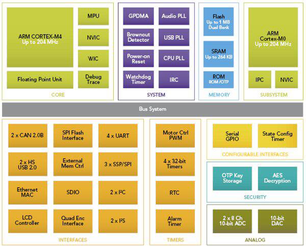
While design teams can use both cores for computational tasks, NXP envisioned a usage model where the M0 core serves more like a peripheral on a typical MCU. For example, the M0 core can implement a complete USB or Ethernet interface offloading all processing requirements from the M4. The chip boots the M4 core first and the M4 in turn boots the M0 core.
Cooper added that NXP assumed the M4 would be the master in typical applications, but early customers are using that configuration as well as designs where the M0 assumes the role as master after booting. For example, some applications only need DSP or other performance-oriented computation capabilities sporadically. A design can periodically disable the M4 core when its capabilities are not required and realize much lower system power usage.
Memory architecture
Turning to other areas of differentiation, memory is a significant one. ST, for instance, has stressed the significance of its Adaptive Real-Time (ART) memory accelerator (Fig. 2). ST developed the architecture to maximize performance by minimizing wait states, even as CPU clock speeds significantly exceed the read-cycle time of the integrated Flash memory that is typically used for code storage in MCUs.
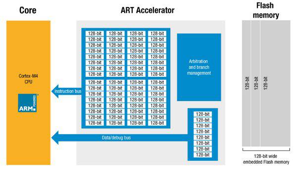
Stuart McLaren, product marketing manager at ST, pointed out that the Flash is organized in 128-bit wide blocks. Because the 32-bit M4 also supports the Thumb and Thumb-2 16-bit instruction sets, there is typically a mix of 32- and 16-bit instructions in memory. McLaren noted that a single memory read delivers four to eight instructions so when the processor is executing instructions sequentially, it does so with no wait states.
The problem occurs when the processor takes a branch in the code or a branch dictated by an interrupt where the processor would incur a wait state to load the new instruction line from Flash. The ART includes 64 128-bit branch caches to handle the majority of such occurrences. The concept is the opposite of how cache is used with microprocessors. High-end microprocessors execute from cache the majority of the time to avoid wait states. The ART only uses the cache to mitigate a penalty on branches.
ST has published benchmarks that show essentially zero-wait-state performance to the current maximum 168-MHz clock rate and beyond. McLaren said, "We believe the ART Accelerator is efficient and the benchmark numbers support that."
The ART Accelerator is deployed across the F2 and F4 ST MCU lines. For now, the available F4 processors include the STM32F405 and STM32F407 products. The features include dual USB ports with high-speed (280 Mbps) and On-The-Go (OTG) operation supported. The DSCs include three A/D Converters (ADCs) and dual D/A converters (DACs). The STM32F407 adds Ethernet support, a camera interface and other features.
NXP, for now, is not shipping any M4-based DSCs with integrated Flash. Neither the current LPC4330 and LPC4350 MCUs nor forthcoming parts due shortly include Flash. Instead, NXP integrates what it calls a Quad SPI Flash Interface (SPIFI – pronounced spiffy) that provides a four-line interface to external SPI serial Flash.
According to NXP's Cooper, the external memory allows design teams to choose the exact amount of memory required for an application, optimizing cost. He noted that many of the media-rich applications for which the M4 is destined will require more memory that can be integrated on chip in any case. Cooper added that depending on the code, the external-memory architecture can offer 60 percent of zero-wait-state performance.
Still, NXP will ultimately introduce models with integrated Flash. Cooper pointed out that its M3-based products with Flash use a 256-bit interface to minimize wait states. Ultimately, design teams will have to balance the choice of an MCU with Flash compared to a design with external Flash in terms of cost, power, footprint, and other characteristics.
Simultaneous data transfers
Freescale does integrate Flash on its currently available Kinetis K10, Kinetis K20, Kinetis K30, Kinetis K40, and Kinetis K60 MCUs as well as the K50 and K70 DSCs that are due to be released soon. Bock said that Freescale uses techniques such as speculative fetches to optimize performance. He also said, "What matters more is the ability to do more than one thing at a time" meaning the ability to simultaneously move data between peripherals, memory, and the core.
Freescale integrates 3 x 3 or 4 x 4 cross-bar switches on its Kinetis family. The matrix will allow, for example, the core to fetch instructions simultaneously with data moving on and off chip, and between peripherals and memory on chip.
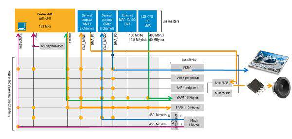
ST and NXP tout similar capabilities. For example, the ST M4-based MCUs utilize the ARM AMBA (Advanced Microcontroller Bus Architecture) High-performance Bus (AHB) designed to link peripherals and memory on chip. Figure 3 depicts what ST calls a multi-AHB bus matrix that is essentially a switch fabric with the CPU, DMA controllers, Ethernet, and USB all having bus-master capabilities. The different colored data flows in the figure can all happen in parallel. The depicted example includes the CPU fetching instructions and data and decoding audio data stored in RAM. The DMA controllers simultaneously output decoded audio as well as graphics images.
NXP's LPC4300 family must add communications support for the second CPU core, as well as the peripherals and external memory. The design relies on segmented memory allowing both cores private access to resources along with a dedicated interprocessor communications block.
Leveraging dual cores
Clearly, the DSC makers are trying to balance processor performance, memory-access speed, and data movement. NXP uses the extra core to spread the processing load, furthering the capacity for simultaneous operations. Cooper uses an audio example to illustrate the capabilities (Fig. 4).
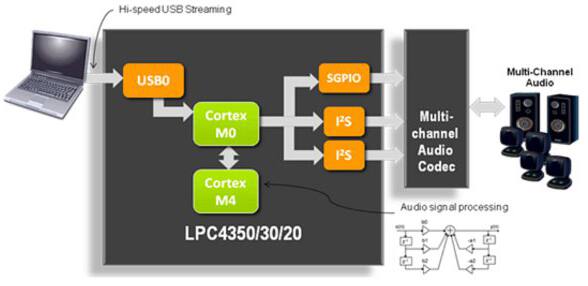
The M4 core in a DSC could certainly handle the task of running both a USB stack and audio processing. However, the USB processing would impact the bandwidth of the M4 for audio, according to Cooper. He said that a typical M4 CPU could handle high-quality 2-channel audio, but by moving the USB processing to the M0 core, Cooper said that the LPC4300 DSCs can handle 7.1-channel audio. Cooper said, "The M0 is perfectly capable of doing any data-handling tasks." Typical usages include programmable I2C and I2S peripherals in addition to USB. Indeed, the audio example uses the I2S capability to output the processed stream.
Peripherals target applications
The final piece of the DSC puzzle is the peripheral mix. In the case of NXP, the M0 core is part of that picture. Moreover, the M0 core can work with the Serial General-Purpose IO (SGPIO) block to create the interfaces mentioned previously and leverage integrated shift registers to generate complex data patterns with little impact on core CPU cycles.
NXP also integrates the USB physical interface (PHY) on its LPC4330 and LPC4350 DSCs, whereas many MCU and DSC USB implementations require an external PHY. Both of the above ICs also include Ethernet support, and the latter adds an LCD controller.
Freescale believes that the analog peripheral set implemented across the Kinetis family differentiates its products. For example, the family includes 16-bit ADCs whereas other vendors max out at 10- or 12-bit ADCs. Freescale also offers 12-bit DACs, programmable gain amplifiers (PGAs), and support for touch-sensing applications.
One other major area of difference is the choice of integrating an FPU. ST and NXP, with M3-based products that in some cases omit an FPU, are for now including the FPU on all M4-based products. The companies assume customers will chose the M4 core for math-centric applications and therefore will want the FPU.
Freescale offers versions of its Kinetis DSCs with and without the FPU, up and down the product line. Freescale's Bock said that unlike the DSP capabilities, the FPU is not a trivial addition even in a 90 nm process in terms of silicon real estate, and therefore cost, or in terms of power consumption.
Freescale also offers a Low-Leakage Wake-Up Unit that expands the operating modes inherent to the M4 core. Together the omission of the FPU and the low-power modes result in DSCs that can operate from coin cells with a current draw under 100 nA when running at 32 kHz.
Security and reliability
The peripheral mix can also come to play in terms of system security and reliability. For example, the Kinetis K60 family has Freescale's DryIce functionality that monitors voltage, temperature, and other conditions that could prove harmful to reliable operations. The high-end processors also include tamper-detection features, a random number generator, and a hardware-encryption processor (Fig. 5) for secure data transmission and storage.

ST has also announced security capabilities for two new ST32F4 family DSCs due soon. The features will include a crypto/hash processor and a random number generator.
In Summary
The growing universe of ARM-Cortex-based MCUs makes the technology an attractive choice for embedded design teams. You have a wide selection of development tools available from the IC vendors and third parties for the software-compatible cores. Additionally, within each semiconductor vendor, the families generally include compatible peripherals making the MCUs software compatible at the system level.
Addressing the ARM trend, Freescale's Bock said, "It's hard to deny the market pull that ARM is capturing in the industry."
Design teams now have a broad range of choices in DSP-enabled Cortex-M4 products to go along with the earlier ARM-based offerings. As we discussed here, the mix of peripheral and memory choices can support most any application. Moreover, design teams can develop scalable products with pin and software compatibility.
免责声明:各个作者和/或论坛参与者在本网站发表的观点、看法和意见不代表 DigiKey 的观点、看法和意见,也不代表 DigiKey 官方政策。


