Device Thermal Coupling on a PCB
投稿人:DigiKey
2015-05-13
The objective of any thermal solution is to ensure that a device’s operating temperature does not exceed the safe limits defined by its manufacturer. In the electronics industry, this operating temperature is referred to as the device’s “junction temperature.” In a processor, for example, this term literally refers to the semiconductor junction where electrical power is converted to heat.
To maintain operation, the heat must flow out of the semiconductor at such a rate as to ensure acceptable junction temperatures. This heat flow encounters resistance as it moves from the junction throughout the device package, much like electrons face resistance when flowing through a wire. In thermodynamic terms, this resistance is known as conduction resistance and consists of several parts. From the junction, heat can flow toward the case of the component, where a heatsink may be located. This is referred to as ΘJC, or junction to case thermal resistance. Heat can also flow away from the top surface of the component and into the board. This is known as junction-to-board resistance, or ΘJB.
ΘJB is defined as the temperature difference between the junction and the board divided by the power when the heat path is from junction to board only. To measure ΘJB, the top of the device is insulated and a cold plate is attached to the board edge (Figure 1). This is the true thermal resistance, which is the characteristic of the device. The only problem is that in a real application one does not know how much power is being transmitted from different paths.

Figure 1: Cross-section illustration of a ring-style cold plate RΘJB 2.
ΨJB is a measure of the temperature differential when multiple heat transfer paths are used, such as the sides and top of the component as well as the board. These multiple paths are inherent in an actual system and measurements must be used with caution.
Due to the multiple heat transfer paths within a component, a single resistance cannot be used to accurately calculate the junction temperature. The thermal resistance from junction to ambient must be broken down further into a network of resistances to improve the accuracy of junction temperature prediction. A simplified resistor network is shown in Figure 2.

Figure 2: Junction to ambient resistor network.1
Prior work done by Joiner et al.1 correlates ΘJMA to board temperature (see Equation 1). The ΘJMA is the overall thermal resistance from the junction to the ambient when all heat transfer paths are evaluated. In this case, ΘCA is represented by the heatsink thermal resistance, as well as the interfacial resistance between device and sink.
Table 1 lists JEDEC parameters for a typical BGA component. These are used in the following example calculation:
ΘJMA = Junction to moving air thermal resistance
ΘJB = Junction to board thermal resistance
ΘJC = Junction to case thermal resistance
ΘCA = Case to ambient thermal resistance
TBA = Board temperature rise
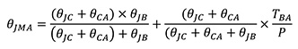 (1)
(1)
| Parameter | Description | Value | Units |
| ΘJC | Thermal resistance - junction to case |
0.45 | °C/W |
| ΘJB | Thermal resistance - junction to board |
2.6 | °C/W |
| TDP | Thermal design power | 20 | W |
| Tj | Maximum junction temperature | 105 | °C |
Table 1: Typical thermal package specifications
As board layouts become denser, there is a need to design optimized thermal solutions that use the least amount of space possible. Simply put, there is no margin to allow for over-designed heatsinks with tight component spacing. Accounting for the effect of board coupling is an important part of this optimization. The possibility for using an oversized heatsink exists only if the junction to case heat transfer path is considered.
To ensure a 105°C junction temperature at 55°C ambient, a typical component (see Table 1) needs a heatsink resistance of 2.05°C/W (if we ignore board conduction). When board conduction is taken into account, the actual junction temperature could be as low as 74°C, assuming the board temperature is the same as the air temperature. This indicates a heatsink that is larger than necessary.
From this example, it is clear that all heat transfer paths from the component junction must be considered. Using just the ΘJC and ΘCA values can lead to a larger than optimal heatsink and may not accurately predict operating junction temperatures. Using the proposed correlation can also predict junction temperature when the board temperature is known from experimentation, as shown in Figure 3.

Figure 3: Effect of board temperature rise on junction temperature.
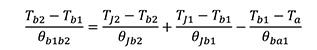
When there is more than one component, the situation becomes much more complex than with just a single component on the board. There is conduction coupling between components through the PCB, and radiation and convective coupling between the components and adjacent cards. A simple PCB with two components is shown in Figure 4. The power dissipation of the two components is assumed to be P1 and P2, and it is assumed that we can neglect the radiation heat transfer. The board temperature under each device is Tb1 and Tb2, respectively. We also assume that the lateral resistance between the two components on the board is θb1b2.

Figure 4: Simple schematic of a PCB with two components.

Figure 5: Simple resistor network of the PCB with two components.
Applying the energy balances at the nodes J1, J2, b1 and b2 :
![]() (2)
(2)
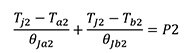 (3)
(3)
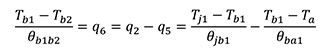 (4)
(4)
 (5)
(5)
There are four equations and four unknowns: Tj1, Tj2. Tb1 and Tb2. The unknowns can be determined by solving the simultaneous equations. This simple example demonstrates that by coupling two components through a conduction path, it becomes much more complicated to find the junction temperatures. In a real-life application, the situation is much more complicated than the above example when encountering multiple components and multiple PCBs with different conduction planes all interacting through conduction, convection, and radiation.
To obtain reasonable answers it is necessary for the designer to use sound engineering judgment in approximating the coupling between different components. This can be achieved by the following methods:
Method 1 - Analytical models, using either a control volume method or a resistor network model. This method requires oversimplification of the problem; otherwise the solution becomes very complicated and impractical.
Method 2 - Use of CFD on a simplified geometry, as described by Guenin [4]. This method suggests that an equivalent surface area for a component is found as:
![]() (6)
(6)
Where An is the equivalent footprint area of the componentn, Pn is the power dissipation of the componentn, PTotal is the total power dissipation and ATotal is the total surface area of the PCB. After the equivalent footprint area is calculated, a simple PCB with a single component having the footprint area An and power dissipation of 1 Watt can be simulated using CFD. This process effectively calculates the difference between the board temperature and the ambient (θBA) for a 1 Watt power dissipation. Figure 6 shows the CFD simulation on one such component and Figure 7 shows the θBA as a function of PCB size. Figure 7 can be used to determine the θBA for other components by simply calculating their effective footprint area. It is assumed that all components have the same footprint size.

Figure 6: CFD simulation of a single component on a PCB [4].

Figure 7: ΘBA distribution as a function of PCB size 4.
The board temperature can then be calculated as:
![]() (7)
(7)
The junction temperature can then be calculated as:
![]() (8)
(8)
Where ψJB is the characterization parameter.
Method 3 - Measure the board temperature, TB, experimentally, if the PCB is available, and use Equation 8 to find the junction temperature. Again, this is an approximation, as the conditions under which the device is coupled to the PCB might be totally different than those used with the JEDEC test board.
This article first appeared in the Qpedia Thermal eNewsletter in December, 2007.
References:
- Joiner, B., Adams, V, Measurement and Simulation of Junction To Board Thermal Resistance and Its Application in Thermal Modeling, Semiconductor Thermal Measurement and Management Symposium, 1999.
- JESD51-2, Integrated Circuits Thermal Test Method - Natural Convection, JEDEC, March 1999.
- JESD51-6, Integrated Circuit Thermal Test Method - Forced Convection, JEDEC, March 1999.
- Guenin, B., Characterizing a Package on a Populated Printed Circuit Board, Electronics Cooling Magazine, May 2001
免责声明:各个作者和/或论坛参与者在本网站发表的观点、看法和意见不代表 DigiKey 的观点、看法和意见,也不代表 DigiKey 官方政策。