Thermal Optimization of GaN HEMT Transistor Power Amplifiers
投稿人:DigiKey
2012-12-06
Gallium nitride power transistors have very high RF power densities which range from 4 to 12 watts per mm of gate periphery, depending on operating drain voltage. Even though GaN/AIGaN on SiC substrates have high thermal conductivity, it is necessary to be aware of channel temperature rise incurred by both DC and RF stimuli when designing power amplifiers. Thermal management is even more important for broadband amplifiers (a very popular application), where drain efficiencies can vary considerably as a function of frequency.
A new self-heating feature in Cree's GaN HEMT large-signal models automatically affects both DC and RF parameters as a function of transistor drawn current. We will use the CGH40025F transistor in a 2 to 6 GHz broadband amplifier and demonstrate how the transistor operating temperature can be minimized during the simulation phase of the design. The default thermal resistance is set for the CGH40025F at 4.8°C/watt. The operating case temperature (Tease) is user defined. The self-heating engine automatically calculates the rise in temperature (Trise) of the HEMT channel above Tease.
Trise can be used as a function of other parameters such as frequency, output power, and efficiency. This article will show the direct lowering of Trise using optimization in unison with the maintenance of output power. Such thermal optimization assures reliable operation as well as improved performance since the transistors are operating cooler.
Basic amplifier design
2 GHz to 6 GHz demonstration amplifier simulation
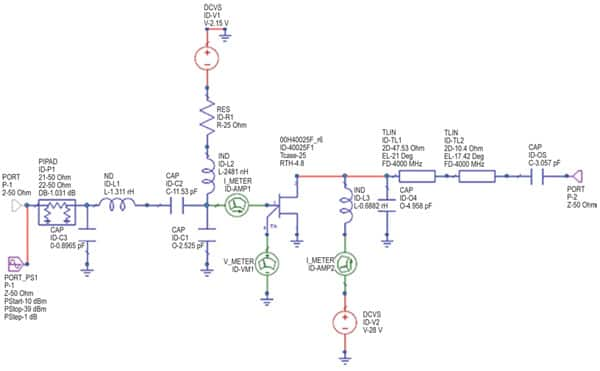
Figure 1: 2 to 6 GHz, 25 W broadband PA schematic.
Figure 1 shows the basic schematic of a broadband, 2 to 6 GHz power amplifier utilizing a Cree CGH40025F GaN HEMT transistor. This device operates from a nominal 28 volt rail. The transistor symbol in the schematic shows a four port device - gate, drain, source and temperature monitor - a voltmeter serves as the "thermometer".
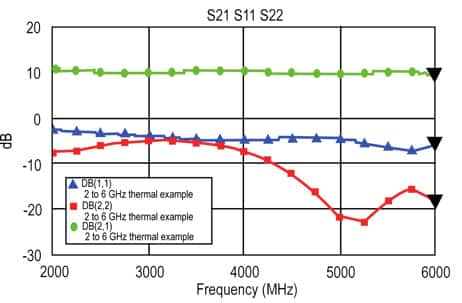
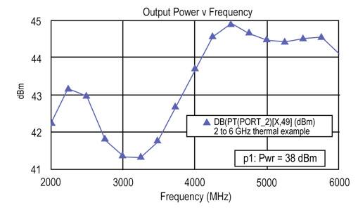
Initial circuit design was concentrated on achieving broadband and flat, small-signal gain across the required frequency range (Figure 2). The power transfer characteristics of the amplifier were then simulated. For example, at a constant CW input power of 38 dBm the output power is plotted as a function of frequency in Figure 3 where it can be seen that the output power varies somewhat due to different levels of compression and impedance match.
Simulated performance prior to optimization
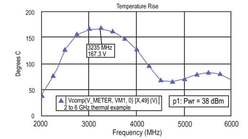
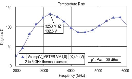
The self-heating feature of the large-signal model automatically calculates the thermal rise in the transistor from package flange to channel. This is shown in Figure 4 for the amplifier before any specific attention has been taken to decreasing operating drain current. Optimization parameters were set up in Microwave Office for output power, gain and temperature rise as a function of frequency. The intention of the optimization is to ensure that the transistor's channel temperature never exceeds 225°C at a case temperature of 85°C (i.e., a temperature rise of 140°C).
Following thermal optimization, the small signal parameters are re-simulated as shown in Figure 5, where there is little change in gain and some improvement in output return loss. Figure 6 shows the CW output power as a function of frequency- again there is general improvement in output power over the band even though the "profile" has changed.
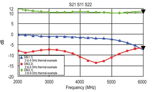
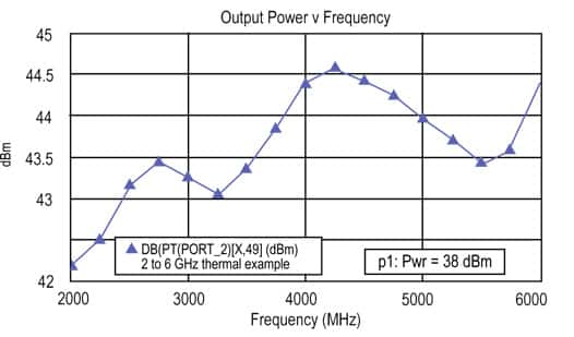
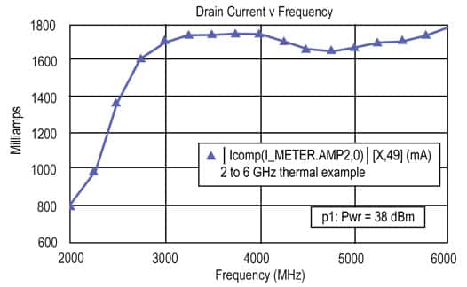
Figure 7 is a plot of transistor drain current as a function of frequency which indicates drain current reduction of as much as 12% compared to the original design. Figure 8 indicates the temperature rise after thermal optimization showing temperature decreases of as much as 35°C compared to the original design.
This article has shown a demonstration of how to use the self-heating feature of Cree's large-signal GaN HEMT models to calculate transistor temperature rise as a function of other parameters such as frequency and RF power level. Specifically, the self-heating engine has been used, via optimization, to lower transistor temperature by minimizing Trise while maintaining output power.

免责声明:各个作者和/或论坛参与者在本网站发表的观点、看法和意见不代表 DigiKey 的观点、看法和意见,也不代表 DigiKey 官方政策。

