


Energy Harvesting Power Management for Wireless Sensor Networks in the Smart City
投稿人:DigiKey 欧洲编辑
2017-01-04
The city is the perfect environment for the Internet of Things. Sensors can be employed to provide useful data for many different applications, and the relatively small data packets means the bit rate of the wireless link can be traded off for lower power consumption. This is vital for networks with thousands or even millions of nodes. Projects around the world are looking at ways of harvesting energy from the environment to power these sensor nodes. Solar, thermal, vibrational and even RF energy are all being evaluated as power sources.
This differs from long range wide area networks such as cellular that need to cover sensors that may be deployed across many miles. Here the energy requirements of the wireless link can often preclude the use of energy harvesting sources.
Instead, the city-based nodes may use a range of different low-power wireless protocols ranging from sub-GHz low-power long-range networks (LPWAN) to the 2.4 GHz Bluetooth Smart and ZigBee technologies as well as proprietary mesh networks.
As the energy harvesting sources have variable, low currents, there are highly specialized requirements for the power management unit (PMU) in order to provide the wireless transceiver, microcontroller, and sensor with power.
Despite increasing integration in the PMU, the design of the energy harvesting power supply for such wireless nodes requires attention to the capacitors and inductors to deliver the optimum power.
The Analog Devices ADP5091 PMU can be used to convert DC power in the 6 µW to 600 mW range to cope with the variations from photovoltaic (PV) cells or thermal energy generators (TEGs) for wireless sensor nodes. These devices charge storage elements such as rechargeable Li-Ion batteries, thin film batteries, supercapacitors, or conventional capacitors to provide a steady current for the sensors. This can also supply the higher power required for the transceiver to send the data to a local gateway.
A key element of the design is an internal cold start circuit so that the regulator can start operating at an input voltage as low as 380 mV. After cold startup, the regulator can handle an input voltage range of 0.08 V to 3.3 V and an additional 150 mA regulated output can be programmed by an external resistor divider or the VID pin in Figure 1.

Figure 1: The ADP5091 can handle variable low energy sources such as photovoltaic solar panels and thermal energy generators.
When used with a PV cell, the controller keeps the input voltage ripple in a fixed range to maintain stable DC-to-DC boost conversion at the most efficient point. The dynamic sensing mode allows extraction of the highest possible energy from the harvester with a programmable minimum operation threshold for a quick shutdown during a low input condition.
The charging control function of the device protects the rechargeable energy storage, which is achieved by monitoring the battery voltage with the programmable charging termination voltage and the shutdown discharging voltage. In addition, a programmable PGOOD flag monitors the SYS voltage. An optional primary cell battery can be connected and managed by an integrated power path management control block that is programmable to switch the power source from the energy harvester, rechargeable battery, and primary cell battery.
The switching mode synchronous boost regulator, with an external inductor connected between the VIN and the SW pins, operates in pulse frequency modulation (PFM) mode, transferring energy stored in the input capacitor to the energy storage connected to the BAT pin. The MPPT control loop regulates the VIN voltage at the level sampled at the MPPT pin and stored at the capacitor through the CBP and the AGND pins.
To maintain the high efficiency of the regulator across a wide input power range, the current sense circuitry employs an internal dither peak current limit to control the inductor current. The main boost regulator operation reaches an asynchronous mode via the energy storage controller if the BAT pin voltage is less than the battery terminal charging threshold programmed at the SETSD pin, or stops switching if the BAT pin voltage is more than the battery overcharging threshold programmed at the TERM pin. The boost regulator disables when the voltage on the CBP pin decreases to the threshold set by the resistor at the MINOP pin. In addition, the boost is periodically stopped by an open voltage sampling circuit and can also be temporary disabled by driving the DIS_SW pin high.

Figure 2: The capacitor and inductor values on the pins of the ADP5091 are essential for correct operation in energy harvesting.
To protect the storage element from overcharging or overdischarging, the storage element must be connected to the BAT pin and the system load tied to the SYS pin in Figure 2. The device supports rechargeable batteries, super capacitors, and conventional capacitors and a storage element with a 100 μF equivalent capacitance is required to filter the pulse currents of the PFM switching converter. The storage element capacity must provide the entire system load when the input source is no longer generating power.
If there is a high pulse current or the storage element has significant impedance, it may be necessary to increase the SYS capacitor from the 4.7 μF minimum, or add additional capacitance to the BAT pin to prevent a droop in the SYS voltage. However, increasing the SYS capacitor causes the boost regulator to operate in the less efficient cold start stage for a longer period at startup. If the application is unable to accept the longer cold start time, the additional capacitor can be placed parallel to the storage element.
The boost regulator also needs an appropriate inductor for proper operation. The inductor saturation current must be at least 30% higher than the expected peak inductor currents, as well as a low series resistance (DCR) to maintain high efficiency. The boost regulator is designed to optimize the efficiency and control the switching with a nominal inductance of 22 μH ± 20%.
Low leakage capacitors are required for energy harvesting applications that are sensitive to the leakage current as any leakage from the capacitors reduces efficiency, increases the quiescent current, and degrades the effectiveness of the MPPT tracking algorithm, dominating the source impedance.
A capacitor (CIN) connected to the VIN pin and the PGND pin stores energy from the input source. A minimum of 10 µF is recommended, but for the primary battery, a larger capacitance helps to reduce the input voltage ripple and keeps the source current stable to extend the battery life.
The ADP5091 uses two capacitors between the SYS pin and the PGND pin. A low ESR ceramic capacitor of at least 4.7 µF is connected in parallel to a high frequency, 0.1 µF bypass capacitor which should be as close as possible between SYS and PGND.
To keep the wireless sensors as small as possible, the device uses small ceramic capacitors, but other capacitors can be used as long as care is taken with the effective series resistance (ESR) value. The ESR of the output capacitor affects stability of the LDO control loop and a minimum capacitance of 4.7 µF with an ESR of 1 Ω or less is recommended to provide a stable output.
The transient response to changes in load current is also affected by output capacitance. Using a larger value of output capacitance improves the transient response of the regulated output to large changes in load current.
The voltage stored on the CBP capacitor is regulated by the VIN pin and is sensitive to leakage because the holding period is around 16 sec. As the capacitor voltage drops due to leakage, the VIN regulation voltage also drops and influences the effectiveness of MPPT.
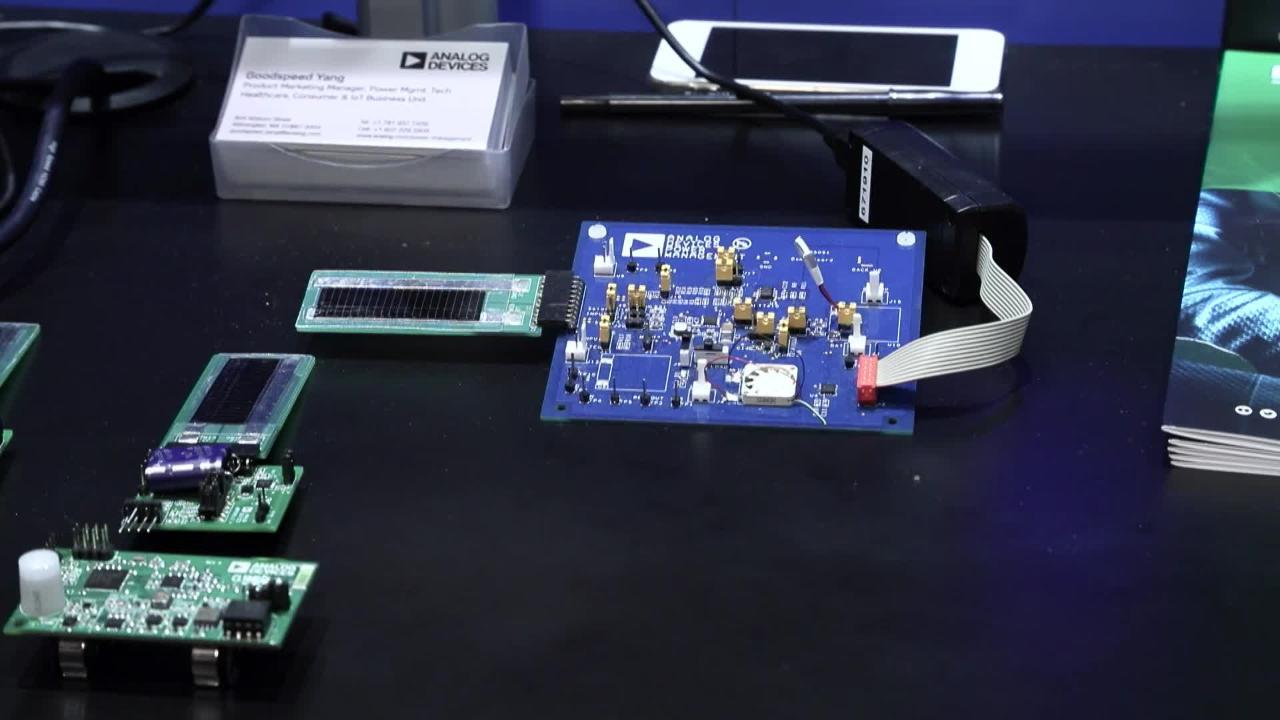
Evaluation board
The ADP5091-2-EVALZ demonstration board in Figure 3 combines the power management device with a PV panel, converting indoor light at 200 to 1000 lux to 0.8 V electrical energy. The ADP5091 boosts the input voltage from 0.8 V to 3.5 V and stores the energy in a supercapacitor.

Figure 3: The evaluation board combines a PV solar cell with the ADP5091 power management unit and connects to a wireless sensor network demonstrator.
This plugs directly into the Analog Devices wireless sensor network demonstrator to link to a low-power microcontroller and sub-GHz long-range, low-power transceiver.
Conclusion
The choice of the capacitor and inductor is vital to the efficient operation of an energy harvesting power management unit for a wireless sensor network. Using small ceramic capacitors allows smaller sensor nodes that can be easily placed both indoors and out to harvest solar energy. This provides data via a wireless link as part of the Internet of Things across the smart city.
免责声明:各个作者和/或论坛参与者在本网站发表的观点、看法和意见不代表 DigiKey 的观点、看法和意见,也不代表 DigiKey 官方政策。


 中国
中国