Hardware vs. Software Tradeoffs – Part 1: Comparators
投稿人:DigiKey 北美编辑
2017-08-22
Editor’s Note: It’s a classic architectural decision: which functions to implement in hardware and which to implement in software. Part 1 of this two-part series will look at design considerations and tradeoffs using comparators as an example. Part 2 will use peak detectors as the example.
It’s easy and somewhat understandable to assume that the best, quickest, and easiest way to implement various basic building block system functions is via a software algorithm and a minimum of “hardware” (circuitry). After all, powerful processors, memory, and analog-to-digital (ADC) and digital-to-analog (DAC) converters are readily available, easy to use, and relatively inexpensive.
Yet the reality is that an all hardware, circuitry-based solution is often the better approach. To arrive at the “best” answer in a given situation, designers need to consider the tradeoffs among many design factors and performance objectives. This article will explore the perspectives from the point of view of the ubiquitous comparator, both with and without added hysteresis.
Begin with a basic comparator circuit
The comparator is widely used from near DC to RF, and across many types of systems and applications. It has a very simple functional description and can be realized with what seems to be simple circuitry or a few lines of code.
Conceptually simple, it looks simultaneously at two analog signals as its inputs, one of which is usually a reference signal (Figure 1). It presents a high (logic 1) output if a signal is greater than the other, and presents a low (logic 0) output for the opposite case (Figure 2).
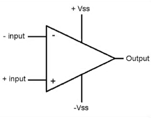
Figure 1: The symbol for the comparator function is very simple, as is its function; it shows the two inputs, one of which is often (but not necessarily) a relatively static threshold value. (Image source: ElProCus)
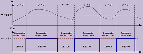
Figure 2: In this basic, typical application, the comparator turns an LED on or off via its 5 volt output as the input signal goes below or above the 2.5 volt threshold. (Image source: ElProCus)
In many, but not all situations, one of the two input signals is not an unknown signal, but is instead a fairly static threshold, limit, or alarm value to which the second signal is being compared. In other cases, comparators are used to select the preferred signal in a diversity antenna or multiple-input/multiple-output (MIMO) receiver scenario, to judge which of two (or more) dynamic signals is stronger and thus preferred.
They are also used in physically compact situations, such as hard disk drives (HDDs) to decide in real time if the distorted, varying and oddly shaped signal from the disk platter’s read head represents a 0 or a 1, with the decision threshold either fixed in advance or adjusted dynamically by a read-channel algorithm.
Hardware implementation of comparator
An analog comparator is simple to implement using an op amp. Although it can be done, it is generally not good design practice to use a standard linear-gain op amp, as issues of open-loop gain, stability, and other subtleties will adversely affect performance. Instead, an op amp which has been specifically designed as a comparator is a better choice. These are called out separately in vendor component selection listings.
There are hundreds if not thousands of comparators offered by vendors. A representative comparator is the CMP401 from Analog Devices, Inc. (Figure 3, top). This low-power device comprises two stages: an analog input stage which can operate from a single +3 volt supply up to a bipolar ±6 volt supply, followed by a digital output stage compatible with 3/5 volt logic.
A key performance parameter is propagation delay, which specifies how long it takes for a change in input state to appear at the output. For the CMP401, this delay is just 23 nanoseconds (ns), as seen in the scope display of Figure 3.
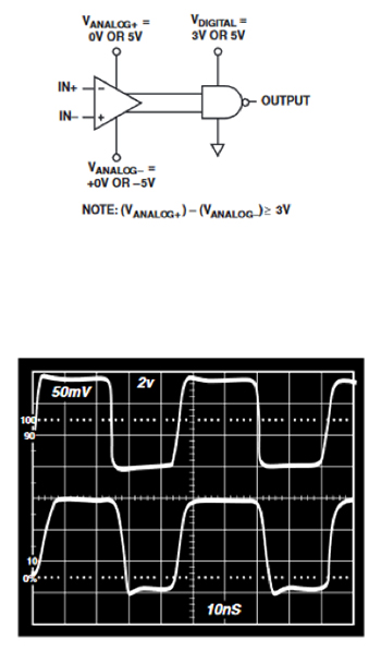
Figure 3: Due to its two stage design, the CMP401 comparator from Analog Devices can handle analog signals having a different range than the digital logic output (top); the propagation delay for a 20 MHz signal is just over 20 ns (bottom). (Image source: Analog Devices, Inc.)
Some “alarm” comparator designs include latching, where the comparator output stays at the triggered level even if the input signal goes back below the threshold. Latching the output serves multiple purposes. Most importantly, it ensures that the output state change can still be seen by the system and processor, even if the comparator inputs revert to pre-threshold values.
Using this approach, the processor can scan the comparator output periodically rather than having it interrupt the processor. Further, it means the alarm output will not go on and off as the inputs change, which would be annoying and also burden the system processor and software. This latch is deliberately cleared by the system software via a reset line that is built into the latch function.
Even if a true comparator is used rather than an op amp, this circuit still has a potential shortcoming. When the signals are very close to each other, the output will toggle back and forth at high speed as the signals undergo their routine, minute variations. In doing so, the comparator output will correctly, but annoyingly, oscillate between a high and low state.
This can be very disruptive to the system as it will keep indicating that an alarm condition is being exceeded/not exceeded, and keep interrupting the system processor for a response. Further, even if the two signals do not have these normal minute variations in their values but are just very close to each other, the inevitable signal and component noise due to layout, EMI/RFI, and other causes will stimulate continuous chatter on the comparator output.
Fortunately, there is a simple circuit solution: adding hysteresis to the comparator circuit (Figure 4). For simplicity, assume one input to the comparator is fixed, and the other is the unknown signal.
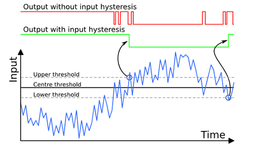
Figure 4: Hysteresis adds upper and lower thresholds, on either side of the original threshold, which the signal of interest must exceed (or go below) before the comparator output changes state, even if the signal passes the threshold itself. (Image source: The Lab Book Pages/UK)
With hysteresis, if the unknown signal is below the fixed threshold value, the output will not change until the signal goes above the threshold by a certain amount (which is set by the component values) and crosses an upper threshold limit. Similarly, if the signal is above the threshold, the comparator will not change output state until the signal goes below the lower threshold by that same amount (Figure 5).
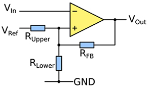
Figure 5: By adding a pair of resistors to the comparator, both upper and lower hysteresis bounds are established; the ratio of these resistors determines the amount of hysteresis using a simple equation found in application notes and handbooks. (Image source: The Lab Book Pages/UK)
Typically, the hysteresis band is set at between 1% and 5% of full-scale range. Although hysteresis is used with almost all comparators to minimize chattering, deciding on its value is a classic engineering tradeoff. If it is set too tight, there may still be too much chattering; if it is set wider to further reduce chattering, some legitimate events may be missed until it is too late. Note that in some designs, the fixed resistors are replaced with software-controllable resistors (digital potentiometers) allowing the system processor to change the hysteresis band as needed.
Regardless of the comparator specifics, this hardware-based approach has several virtues:
- It operates independently of the system processor and so places no burden on that resource, except when there is a comparator output transition signaling the processor via an interrupt or digital I/O.
- It is reliable and contributes to system integrity since the high/low decision is made without any software intervention, making it attractive for safety related alarms. In some systems, the output of the comparator is actually hard wired to an alarm indicator or lamp.
- The circuit can handle fast-changing, wideband signals, and its response is limited only by the comparator’s speed; comparators which can handle gigahertz range signals are readily available.
Software alternative to hardware comparator
A circuitry-based comparator function is effective, but it has costs in terms of pc board space, components on the BOM, and relative lack of adjustability. An alternative approach uses software-based signal processing and leverages circuitry that may already be in place.
In concept, the process is simple. The signals to be compared are first digitized, which likely needs to be done anyway for the system function. Note that if there is only one external input and the other input is a threshold value set by the program, then only that one external input signal needs to be digitized.
Next, the software performs a simple “compare” of the digitized values or the single value versus the threshold number, decides which signal is larger, and sets an output flag to 1 or 0. It then repeats this process over and over (Figure 6). In a practical design, there’s also an additional up-front task of implementing a weighted average on the digitized signal or signals before the comparisons. This minimizes the effects of ADC quantization error and least significant bit (LSB) jitter.

Figure 6: The core of the comparator function can be implemented in software with a relatively simple program that follows a straightforward flowchart. (Image source: DigiKey)
While the flowchart for a comparator’s program code is straightforward, the final program will have additional code to check for special situations and error conditions. Most designs use some averaging of the input samples to reduce the effects of input signal and ADC quantization noise.
The question now becomes, “How fast does this small software loop have to cycle to ensure it doesn’t miss digitized samples, and thus a change in signal status?”
The Nyquist theory serves up the answer: At a rate equal to the digitization, which itself should be done at least twice the highest frequency of the signal. In practice, the sampling rate is typically five times the highest frequency to overcome noise, jitter, and other digitization artifacts. The result is a small software loop running at a rate commensurate with the Nyquist rate of the signal.
Similar to the hardware-based approach, a simple comparison in software results in chatter on the output. Therefore, the simple flow chart must be expanded to add a hysteresis function (Figure 7). In the software version, the hysteresis value can easily be changed as needed, which is an advantage over the hardware approach.
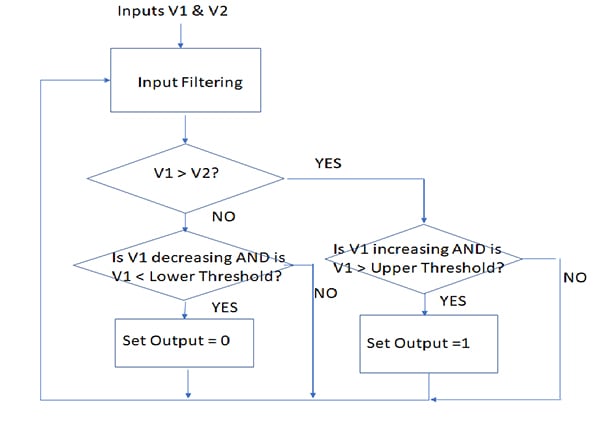
Figure 7: Adding hysteresis requires more code to implement the additional comparisons as shown in the flowchart, but is still a relatively simple program; the final program will have added elements that anticipate and accommodate possible error conditions or artifacts. (Image source: DigiKey)
The hysteresis part of the program must determine two things:
- Is the latest data sample greater (or less) than the previous one?
- Has it crossed the upper (or lower) hysteresis threshold? If the answer to both is “yes”, then the comparator output status should be flipped.
In this way, the code emulates the functions of the op amp based circuitry, but with less hardware and with additional flexibility. However, the code must also include error and false data checking, as well as checking for those improbable or nonsensical events that will inevitably occur with real-world signals. This ensures that noise in the sensor signal, ADC, or circuitry, does not cause false output states.
Conclusion
For a widely used function such as the comparator, designers can often consider both hardware-based and software-based approaches. The software approach requires fewer components and has greater flexibility. However, it is suited to lower speeds and lower update rates.
The all hardware approach gives designers the peace of mind that comes with a familiar device that can be applied across a range of application requirements, from low to high speed. This is particularly important where the A/D conversion and software comparison would require a costly, power-hungry, high-speed converter and fast, highly predictable software loops.
Regardless of approach used, each requires attention to detail to avoid the undesired consequences of signal artifacts, jitter, and other glitches.
免责声明:各个作者和/或论坛参与者在本网站发表的观点、看法和意见不代表 DigiKey 的观点、看法和意见,也不代表 DigiKey 官方政策。


