
Sensor Loops Rely on the Correct Data Converter
投稿人:Convergence Promotions LLC
2013-03-07
As environmental sensors are becoming more widespread in both consumer and industrial applications, it is increasingly important to select the correct data type for the sensors. Most industrial systems operate from line voltage and as a result have plenty of power available for signal processing, thus enabling a low noise floor. This enables the ability to use both higher resolution converters and larger signal processing reference voltages for the sensors. These larger ranges allow for more bits of data to be obtained and tracked.
Consumer systems, on the other hand, are increasingly moving to battery operation, and thus have power constraints that limit the precision, as well as the speed of the data conversion process. Understanding the various types of converter subsystems, and how they affect sensor data, is key to designing real-time M2M systems.
Understanding data conversion
The first step in implementing a sensor system for monitoring and control applications is to understand what sort of data is needed for the system. In most cases, the sensor produces an analog signal as an output. A microcontroller or other, digital logic-based system must process this signal. In order to control a closed-loop system, these logic- and microcontroller-based cores need to have their output converted from digital back to analog in order to drive mechanical systems.
A common misperception is that the resolution of the data converter should be the same as the word size of the microcontroller – 8 bits for an 8-bit micro, 16 bits for a 16-bit micro, etc. However, this not the case. The resolution of the data converter should complement the type and size of the signal measured, as well as the sensitivity of the system to the voltage or current levels of the LSB (least significant bit) of the output from the data converter.
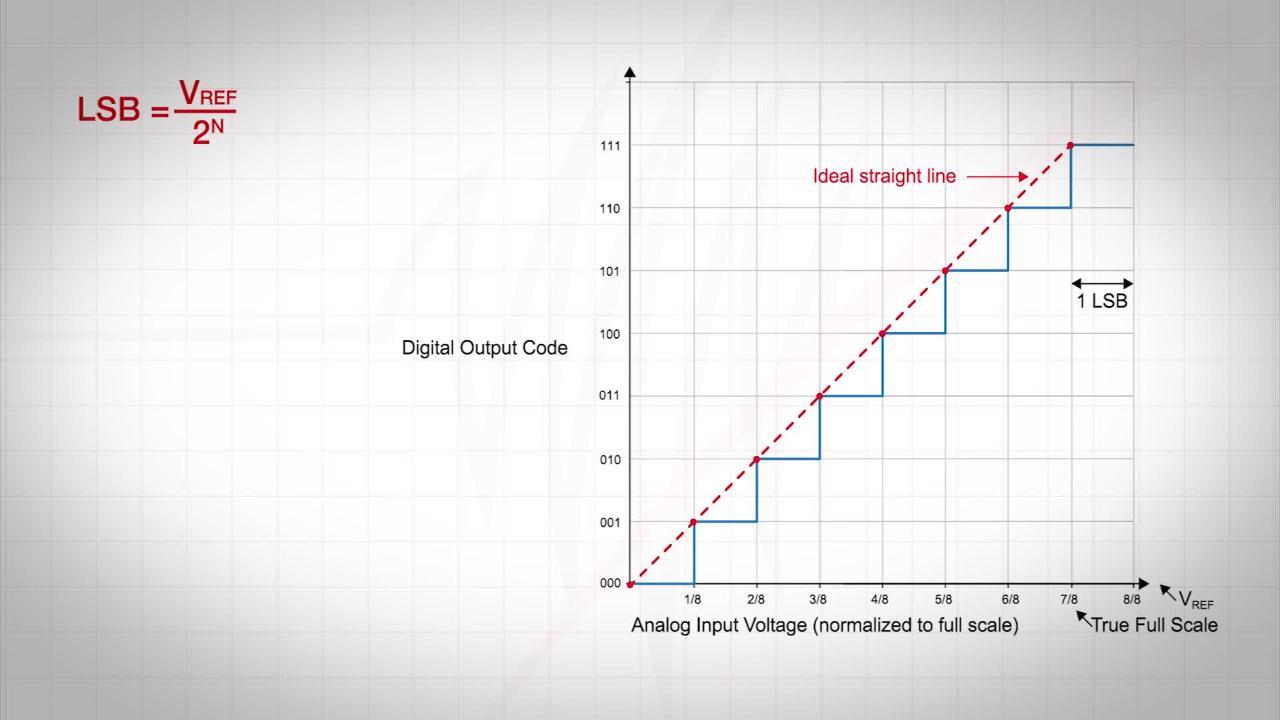
The first step in understanding data converters is to see how the number of bits relates to the size of the measured signal. The Analog Devices Data Converter Fundamentals PTM module shows the relationship between the resolution in bits, the relative size of the steps, and the dynamics involved (see Figure 1). The table below clearly shows how the dynamic range is expanding the rate of 6 dB per bit for either a DAC or an ADC. Most industrial sensors operate on higher voltages, such as a ten volt signal range on a twelve volt supply system, in order to maintain a reasonable signal-to-noise ratio. The figure shows the transition point from workable small steps – mV level in the 10- to 12-bit range to very precise tracking in the μV levels with 16-bit converters.

Power supplies and signals
While the resolution in bits defines the number of steps for the converter, the practical limits on the LSB are dependent on the noise floor and the Full Scale (FS) range for the system. The LSB step size is found by the equation (FS/2n), where n is the number of bits. The FS amount is the voltage distance between the VREF- (all 0 code) and VREF+ (all 1 code) of the system. Most FS ranges are close to ten volts for an industrial sensor application, and about 1.8 to 2.4 V for mobile functions. Industrial and commercial applications have plenty of clean, 12 V supplies available for the main logic setup. These enable the data converted to be accurately sampled within the voltage range of the power supplies. In mobile battery systems, the supplies are in the 3.3 to 5.0 V range, which in turn scales the FS down by more than one volt.
In addition to the range of the data that is collected, you also need to consider the representative information from the frequency of the signal. The ADI training module that included Figure 1 provides an overview the challenges of signal capture and reconstruction by ADCs and DACs. Figure 2 shows how a signal is captured and sampled by an ADC, and then reconstructed by a DAC. The speed of sampling and the settling time of the reconstructed signal are both integral in correctly representing the original waveform that comes from the sensor.

Choosing a data converter with too much resolution, an overly high number of bits, reduces the sampling and reconstruction rates possible in the system. The reduced data rates introduce a risk of aliasing error. Aliasing occurs when the sampling rate is close to the Nyquist bandwidth for the signal being sampled (fa). The sample frequency is denoted as fs. The Nyquist bandwidth is defined to be the frequency spectrum from DC to fs/2. The frequency spectrum is divided into an infinite number of Nyquist zones, each having a width equal to 0.5 fs. The assumption is that for correct capture and reconstruction fs is greater than 2 fa. In practice, the ideal sampler is replaced by an ADC followed by an FFT processor. The FFT processor only provides an output from DC to fs/2, i.e. the signals or aliases which appear in the first Nyquist zone.
Having determined these two basic criteria for converter selection, the next step is to examine the detailed specifications of the converters based on the needs of the sensors. These specifications include rate of change; sensitivity; whether they are processing single-ended or differential signals; whether the sensor information is being used in an absolute or relative change fashion; and the linearity requirements over the temperature range of the sensors. These factors all directly drive the linearity (both integral and differential) specifications of the converter as well as pre- and post-filtering, buffering, and sample-and-hold requirements. The details on these other specifications are explained in the ADI training module, but are further clarified in the Texas Instruments PTM module on Data Converter Basics.
DACs and closing the loop
In closed-loop sensor systems, the output of the digital microcontroller has to be converted back to an analog signal to be used in real-time applications. These devices generally handle motor control, offset trim, and calibration. For most feedback applications, the DACs use a voltage or current reference that is smaller than the full scale of the signals from the sensors. This is the case since it is a correction signal that is being sent, not a full signal.
The Microchip MCP4706 family of DACs is typical in this regard. These parts are available in 8-, 10-, and 12-bit versions with the same pin-out. While designed for full-signal restoration and rail-to-rail output, these devices are typically used with the VREF pin to provide an intermediate full-scale level and a finer degree of control with a reduced LSB step. Figure 3 shows a block diagram of the MCP4706 in its voltage in-and-out mode. Some applications, such as offset control, cannot utilize a voltage output. In those cases, a transconductance amplifier is used on the output of the DAC to help close the loop. An operational transconductance amplifier (OTA), such as the On Semiconductor NE5517DG, is typically used for current-output configurations. These amplifiers are completely self-contained and provide a single or dual signal path for isolated current conversion. Figure 4 shows the block diagram of the NE5517DG OTA.


The advantage of an OTA is the presentation of a uniform loading on the output of the DAC. This allows the system to have a predictable settling time and remain isolated from system noise. It also helps avoid peaking that may result from application of the feedback and calibration signals to the motor control or other environmental/electromechanical system being monitored. Similar to the current output, it is best practice to use a unity-gain voltage follower at the output of the DAC to provide system stability and improved response. Typical DACs have a minimum load resistance level – in the case of the MCP4706A it is 5 KΩ – for the output to be stable. The use of external amplifiers allows for driving lower-impedance nodes.
Data capture through analog-to-digital conversion
Sensor systems generally produce voltages or currents as a measurement of their current environmental condition. To be able to process these inputs in an automated fashion, they need to be converted into a digital representation. These measurements are quantized or captured in both the time and frequency domains. The temporal aspect of the continuous signals is one of the key points in determining the type of ADC to use. The three primary types of ADCs are Flash, successive approximation, and sigma-delta.
Because of the Flash architecture and its derivatives, the multi-stage Flash and pipeline converters are the fastest method. This is a parallel configuration where the sampled signal appears at the top of a reference string. There are multiple simultaneous circuits that all check if the magnitude of the signal is greater than their reference voltage. In this method, the time delay for a sample is one device path (a comparator and latch). The drawback is that for high resolution you need 2n comparators for an n-bit converter. This large parallel configuration not only consumes a great deal of power, but it is also a very heavy capacitive load on the signal being sampled. In order to speed up the converter, the reference resistor string is designed to have a minimized resistance, which may cause a problem for the sensor to drive such low impedance without impacting the performance of the sensor.
A typical multistage Flash converter is Texas Instruments’ TLC0820AIDW as shown in Figure 5. This 8-bit converter combines two 4-bit Flash converters with an embedded DAC to balance the two-step approach. It provides a worst case 2.5 μsec conversion time with a 1.18 μsec average. The device targets fast moving signals up to 100 mV/μsec, and can capture the signals in as little as 100 ns. To support this signal capture, the device has a built-in track-and-hold amplifier. This amplifier is tuned to the load of the ADC sub-sections, isolating the input signal from the clocking and switching of the two sub-converters and the DAC.

The Texas Instruments ADS1131 sigma-delta converter (see Figure 6) has a high gain (64), built-in input amplifier. Due to the slow sample rate of 10 or 80 samples per second, the design needs to use an external sample-and-hold amplifier for standard operating mode. The device has a third-order modulator and a fourth-order digital filter that operates at a sample rate of 76.7 kHz. This relatively high sample rate for the signal processing allows the device to produce the effective tracking resolution when used in continuous conversion mode. The output of the device is in binary two’s complement format, available to the external microcontroller on a continuous stream basis since the device does not need a storage-register bank to load full-conversion outputs.

A similar sigma-delta device is Microchip’s MCP3422 (see Figure 7). This device has a resolution that is dependent on the sample rate. At 24 samples per second, the device can produce 12 bits of resolution and up to 18 bits of resolution at 3.75 samples per second. The MCP3422 features an I²C interface, single-supply operation, and a programmable-gain amplifier at the input. The PGA range is one to eight and the device incorporates its own voltage reference.

The successive approximation converter from ADI (see Figure 8) is designed for high sample-rate, high-resolution data conversion. This converter gives full-scale adjacent sample results at 1 Msps, and only requires a sample time of 290 ns to acquire the signal. The device is designed for use in applications where the result of the signal acquisition is a new, unique 18-bit code for every sample. Rather than having a continuous mode, this device resembles Flash converters and is bound by the Nyquist criteria for the sample rate. Driving this part requires a differential input. Some sensors provide a single-ended output that needs to be converted to differential with a very low offset and distortion. Specialized drivers such as Analog Devices’ ADA4941-1 have been designed for the specific purpose of driving high-resolution ADCs. These amplifiers have a very short path delay and a high impedance output stage to allow for minimal interference with the signal prior to sampling.

Figure 8: Analog Devices’ AD7982 ADC block diagram. (Courtesy of Analog Devices.)
Designing a sensor interface to data converters requires understanding the signal type and the use model of the data that is output from these converters. Selection of the proper technology types allows for full closed-loop automated control of the sensor systems.
免责声明:各个作者和/或论坛参与者在本网站发表的观点、看法和意见不代表 DigiKey 的观点、看法和意见,也不代表 DigiKey 官方政策。