A Simple Approach for Harvesting Energy from Indoor Lighting
投稿人:DigiKey 北美编辑
2017-06-20
Solar energy harvesting offers a practical solution for powering connected sensors, control nodes, IoT devices, and other embedded applications. It can, however, be difficult to extract sufficient energy from a solar cell that needs to accommodate the small form factors of these applications.
Unlike large energy harvesting applications, energy harvesting for these designs typically yields miniscule amounts of power. Designers face multiple challenges in developing subsystems capable of operating at what are often microwatt levels. However, by using power management ICs (PMICs) from Cypress Semiconductor, engineers can rapidly implement energy harvesting power supplies able to operate at these ultra-low power levels.
Limited energy
By harvesting power from ambient energy sources, engineers can create designs that can run indefinitely with no additional power source. For the IoT, this approach is particularly attractive for small, wireless systems that have relied solely on battery power in the past. Using energy harvesting, developers can eliminate batteries entirely. For more power intensive designs, energy harvesting can substantially extend battery life, largely eliminating the need for periodic battery replacement.
In many designs, a typical solar energy harvesting system requires large solar cells or arrays to provide sufficient power. For tiny sensor systems, however, large solar cells are not suitable due to a desire for compact designs, or limited installation space at the target location.
The need for smaller solar cells further complicates energy harvesting for a typical indoor IoT design. Indoor light sources generate very small illumination levels, ranging from about 100 to 200 lux in a typical home, and from 250 to 500 lux in an office. Even well illuminated areas, such as drafting tables or workshops, offer light levels that are orders of magnitude below sunlight illumination levels.
Solar cell manufacturers have responded to the need for indoor solar cells with technologies such as amorphous silicon. Unlike crystalline silicon used in traditional solar cells, amorphous silicon possesses an irregular structure that absorbs more light than crystalline structures. Constructed from these specialized materials, solar cells such as those in the Panasonic Amorton family can generate power even at very low light levels (Figure 1).
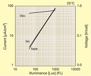
Figure 1: Illuminated by a fluorescent light source, a solar cell designed for indoor illumination exhibits a characteristic relationship between illumination and output as shown here for operating current (Iope), short-circuit current (Isc), and open circuit voltage (Voc). (Image source: Panasonic)
For example, the Panasonic Amorton AM-1801 is a 53 x 25 millimeter cell that generates 4.60 microamps (μA) at 2.6 volts with 50 lux illumination, and 18.5 μA at 3.0 volts with 200 lux illumination. Used in their intended indoor applications, these devices generate output current levels that remain orders of magnitude less than those achieved with solar cells designed for outdoor use (Figure 2).
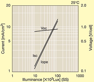
Figure 2: Illuminated by a solar simulator (SS) light source, a solar cell designed for outdoor use generates current output levels that are orders of magnitude higher than those available in indoor applications using indoor cells. (Image source: Panasonic)
For designers, the availability of these specialized cells offers opportunities for energy harvesting designs powered by indoor lighting. The difficulty remains one of creating designs capable of operating at the microwatt power levels associated with these cells, constrained by their expected use in relatively poorly lit indoor locations. Although designers can find ultra-low-power discrete components to build suitable energy harvesting solutions, few designers have the necessary analog design experience to do so. Fortunately, the availability of Cypress Semiconductor’s energy harvesting PMICs allows developers to add ultra-low-power energy harvesting into their designs using only a few support components.
Energy harvesting PMIC
The Cypress S6AE102A and S6AE103A energy harvesting PMICs integrate voltage control circuits, switching circuits, and logic designed to optimize power delivery to the load from a solar cell or optional battery (Figure 3). Designed to operate with a nominal 3.3 volt cell input (or 3.0 volt battery input), the device’s input circuits include an overvoltage protection (OVP) feature that monitors the open circuit voltage of the solar cell to maintain proper operation. To provide a stable output voltage, the device includes a low-dropout regulator (LDO). The LDO regulates the output to within 50 millivolts (max) across a wide range of load current levels. The S6AE103A also includes an independent comparator and timers for more specialized energy harvesting designs.
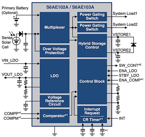
Figure 3: The Cypress Semiconductor S6AE102A and S6AE103A PMICs integrate all the functionality required to harvest energy from a small solar cell, and to switch device output to a battery if harvested energy falls below minimum levels. Additional features (*1 and *2) are available in the S6AE103A. (Image source: Cypress Semiconductor)
Even with its extensive functionality, the 4 x 4 millimeter device nominally consumes only 280 nanoamps (nA) in base operating mode, with another 200 nA required when the LDO is enabled. Just as important, the device needs very little startup power, requiring only 1.2 microwatts. Thus, the device can begin to operate even at the very low power levels generated by indoor cells illuminated with typical room lighting. If insufficient power is available from energy harvesting, the device uses its integrated power supply switching control block to drive the system load from the battery source (Figure 4).
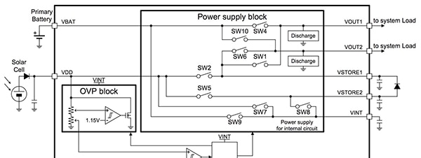
Figure 4: This portion of Cypress S6AE102A and S6AE103A block diagram focuses on the power switching function. The on-chip switches gate power to the system load from the solar cell energy storage capacitor VSTORE1, or from a coin cell if the power available from energy harvesting falls below minimums. (Image source: Cypress Semiconductor)
During operation, the device stores harvested power on a small external capacitor (min 100 µF) at its VSTORE1 pin. In a typical design, the device monitors the cell input (VDD), the battery input (VBAT), and VSTORE1 to determine which source it should direct to its output pins, VOUT1 and VOUT2 (Figure 5).
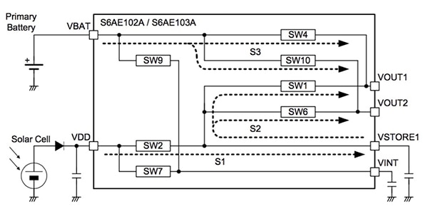
Figure 5: The PMIC power gating control system operates the chip’s integrated switches in combination to route power as needed from the energy harvesting system, or from the battery to the system load at VOUT1 and VOUT2. (Image source: Cypress Semiconductor)
Initially, when VSTORE1 remains below threshold, the device sets its switches to drive VOUT1 and VOUT2 from VBAT (path S3 in Figure 5), while allowing the solar cell to charge VSTORE1 (path S1). When the solar cell input has driven VSTORE1 above threshold, the device switches the load to VSTORE1 (disabling path S3 and enabling path S2) and opens SW2 to disconnect the solar cell from VSTORE1 (path S1). If power stored on the VSTORE1 capacitor is depleted, the device reconnects VBAT to the output (disabling path S2, while enabling paths S3 and S1 in Figure 5).
The device also provides a mechanism for the device to store excess energy harvested from the solar cell. Here, designers would typically place a supercapacitor (min 2 millifarads) on VSTORE2. In this configuration, when VSTORE1 reaches threshold and the device enables path S2 (Figure 5), the device enables a separate switch (SW5 in Figure 4) to allow the solar cell to charge the VSTORE2 capacitor. A diode connecting VSTORE2 to VSTORE1 (see Figure 4) connects the excess energy to the output when VSTORE1 is enabled.
In monitoring VDD and VBAT levels as described above, the device operates in its so-called energy driven mode. The device also offers additional operating modes that allow developers greater control over the power path switching mechanism. In its event driven operating modes, the device utilizes its integrated timer and a control pin (INT) to decouple VOUT1 and VOUT2, routing VDD or VBAT to VOUT2 as appropriate. Using its multiple timers, the S6AE103A supports an additional timer driven operating mode. As with event driven mode, this special mode decouples VOUT1 and VOUT2, but developers can use the S6AE103A’s timers to control power switching separately to VOUT1 and VOUT2 from the supply sources.
Designers set the operating mode and timer duration using combinations of the device’s timer pins, CIN0 and CIN2. The S6AE103A provides an additional timer pin, CIN1, to support its additional event driven and timer driven operating modes.
Along with controlling the output source, developers can fine-tune the final output voltage at VOUT1 and VOUT2 using three resistors arranged as a voltage divider across a pair of control pins, powered by the device’s internal voltage reference source. By adjusting these resistor values, developers can raise or lower the final voltage output within the device’s operating range.
Along with VOUT1 and VOUT2, the device provides an additional voltage output pin, VOUT_LDO, from its internal LDO regulator (Figure 6). As with the device’s VOUT1 and VOUT2 outputs, designers can adjust the LDO output voltage level by setting resistors at VOUT_LDO and FB_LDO pins. An LDO control pin, STBY_LDO, lets engineers switch the LDO between normal mode and a low-power standby mode, reducing LDO power consumption from 6 μA (typical) to 400 nA (typical). An additional device pin, ENA_LDO, allows engineers to enable or disable the LDO entirely.
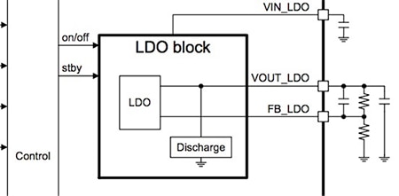
Figure 6: Developers can use a pair of resistors to adjust output voltage (VOUT_LDO) supplied by the low dropout (LDO) regulator integrated in the Cypress energy harvesting PMICs. (Image source: Cypress Semiconductor)
For designers, the device’s use of a few resistors for configuration translates into relatively simple designs based on these PMICs. The 20 pin S6AE102A and 24 pin S6AE103A require few additional components beyond those mentioned to implement an energy harvesting design.
Simplified design using an eval kit
The Cypress Semiconductor CYALKIT-E04 evaluation kit provides a complete energy harvesting system design able to power a sensor system from a small solar cell. Along with a Panasonic AM-1801 solar cell, the kit includes a pair of energy harvesting boards that separately demonstrate designs based on the S6AE102A and the S6AE103A (Figure 7). The separate sensor board connects to the S6AE102A/S6AE103A boards to provide signals from its on-board motion and light sensors, as well as an optional coin cell battery that can serve as the PMIC VBAT source.
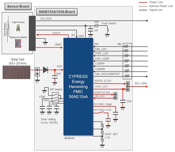
Figure 7: The CYALKIT-E04 evaluation kit includes demo boards for the S6AE102A and the S6AE103A PMICs, showing the few external components designers need to implement a complete energy harvesting design based on either PMIC. (Image source: Cypress Semiconductor)
The PMIC boards also provide Arduino-compatible pin headers for easy connection to the broad portfolio of Arduino add-on boards. Cypress takes advantage of this standard connector to add wireless connectivity using another development kit, the CY8CKIT-042-BLE.
Although beyond the scope of this article, the CY8CKIT-042-BLE add-on board completes the hardware interface shown on the right side of the board in Figure 7. Cypress includes support for this BLE kit in its standard software distribution for the CYALKIT-E04 evaluation kit. For designers, creating a solar powered, wireless sensor design is as simple as connecting the CYALKIT-E04’s sensor and PMIC boards with the CY8CKIT-042-BLE board set.
Conclusion
Energy harvesting can offer an effective solution for low-power designs. In practice, however, few developers have the time or expertise to design energy harvesting circuits capable of extracting the very low levels of ambient energy available. Requiring as little as 1.2 μW to start up, PMICs from Cypress Semiconductor integrate a complete energy harvesting subsystem able to generate useful power from a small solar cell.
This PMIC family requires only a few external components, allowing developers to rapidly implement an energy harvesting power supply from low-level indoor lighting.

免责声明:各个作者和/或论坛参与者在本网站发表的观点、看法和意见不代表 DigiKey 的观点、看法和意见,也不代表 DigiKey 官方政策。
