Droppin’ Traces: Part 3 on PADS Maker/MakerPro
A Three-Part Series Sampling EDA Tools (PCB Design Software)
Being a technician and working at DigiKey can be equated to the quintessential “kid in the candy store,” only for geeks. Having almost instant access to millions of electronic parts and an internet full of example circuits and tutorials leaves the door wide open to creating a plethora of circuits.
Free-form soldering a circuit is fun one time to prototype something, but more than once is crazy if you have the means to spin a board. Once tested, being able to repeatedly drop your parts down and solder, knowing the connections are correct, is priceless (in terms of your sanity and time). EDA = Electronic design automation.
In this third and final part of the series are some of my experiences with PADS Maker/MakerPro.
Using PADS Maker/MakerPro (formerly Designer Schematic & Designer Layout by Mentor Graphics) was hard at first, but I’m no EDA master. Once I learned how to navigate the software better (and having experienced the limitations of other tools), I am realizing what years of EDA prowess the people at Mentor (now part of Siemens) have baked into this. It is really hard to sum up all of the benefits PADS Maker brings in a short blog like this. I encourage you to take the time to learn how to navigate it before giving up too quickly; I believe you’ll be glad you did.
I had a 73 V string of LEDs to light at 120 mA and found this design in our Reference Design Library:

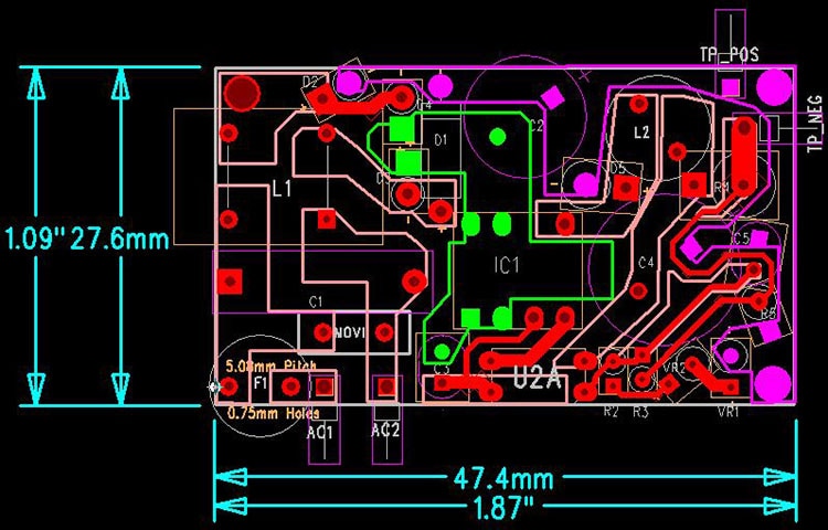
Layout with fill zones (less work for our PCB router/mill):
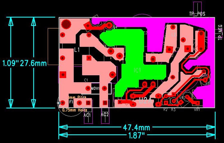
Zones flooded:
Routed and stuffed (yes, having an in-house router is fantastic):
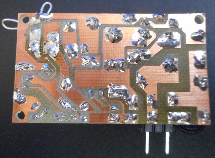
(I know, I still need to clean that bit of flux off; I swapped out the current sense resistor.)
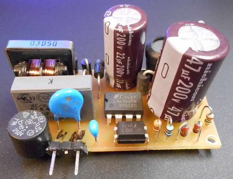
It worked! (low efficiency due to me choosing the wrong inductor)
It is hard to recall all the differences with the tools I’ve used, but I’d be remiss to not point out that PADS Maker can handle almost any font within your PC. Other packages I’ve used give you stroke font, but that’s it.
The fonts came in handy when designing our PCB Layout Reference ruler:
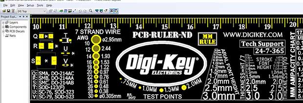

Another feature is a button to flip the image so you don’t need to think in reverse like other the tools do. (A work-around to this issue in KiCad is to keep the 3D view open on another screen and update it after every change—which is not optimal.)
For anyone who has yet to learn to create PCBs (i.e. use EDA tools), there has never been a time like the present. You can learn, design, and order quality PCBs, even in small batches, for a fraction of the price of days’ past.
For those who have used different EDA tools, I hope this series sharing a glimpse into my experiences with easyEDA, KiCad, and PADS Maker/MakerPro was at least entertaining, if not encouraging, should you wish to try something different. Jump in, start simple, leave plenty of space at first, and have some good clean geeky fun.

Have questions or comments? Continue the conversation on TechForum, Digi-Key's online community and technical resource.
Visit TechForum
