Power Amplifiers for Wireless Systems
投稿人:电子产品
2012-04-05
The last output stage in every wireless system includes some form of RF power amplifier (PA) to send the signal to the antenna. Depending on the frequency band the wireless system uses, the power output, and the efficiency desired, designers can select from among power amplifiers fabricated with a wide range of technologies – gallium-arsenide (GaAs), indium-gallium-phosphide, silicon-germanium, bipolar, CMOS, or gallium nitride (GaN). Systems such as cell phones; cordless phones; Wi-Fi, LTE, and WiMAX adapters; wireless routers and access points; wireless cable replacements; base stations; repeaters; push-to-talk radios; walkie-talkies; ZigBee; and Bluetooth all have significant differences in their RF power outputs, frequency bands, efficiency requirements, and cost. Thus, having a wide variety of PA options allows designers to optimize the wireless system to make the best cost/performance trade-off.
For battery-powered systems, low operating and standby currents and high power efficiency are critical requirements, as current consumption and efficiency will significantly impact the system’s battery life. The more efficient the PA, the longer the talk time or the longer a Wi-Fi connection can be sustained. Line-powered systems such as base stations, routers, and access points usually require higher-power outputs and thus have higher active currents. Although efficiency is still important, it is for a different reason. Many of the systems are in sealed enclosures that have minimal air flow, so heat build-up is a significant concern. The higher the efficiency, the less heat dissipated, and thereby better system reliability.
Of all the technologies, GaN High-Electron-Mobility Transistors (HEMT) shows a lot of promise for future system designs. Since GaN devices can operate at high temperatures (and thus can use smaller heat sinks) and handle high power levels, they are ideal candidates for mobile infrastructure systems (base stations) and WiMAX wireless applications. Currently, GaN-based PAs are more expensive than silicon solutions, but GaN’s enhanced performance and ability to operate at high frequencies (> 4 GHz) could bring the cost in line at the system level. Additionally, future manufacturing advances will also further reduce the cost of GaN. Let’s take a look at some of the amplifier offerings across various technologies.
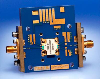
GaN solutions are just starting to be introduced into systems such as electronic countermeasures, radar, and communication systems. One of the first commercial monolithic GaN HEMT power amplifiers, the CMPA0060025F from Cree Inc. delivers 17 dB of small-signal gain and up to 25 W of saturated output power (Figure 1). The monolithic microwave integrated circuit (MMIC) can operate between 20 MHz and 6 GHz at voltages of up to 50 V. The amplifier has a power-added efficiency of better than 20 percent and the input and output ports are internally matched to 50 Ω. Housed in a 0.5 x 0.5 inch screw-down package, the MMIC offers greater power density and wider bandwidths compared to silicon or GaAs transistors. The company also offers a large family of GaN MMICs that meet many power/bandwidth requirements.

GaAs – mainstream technology for power amplifiers
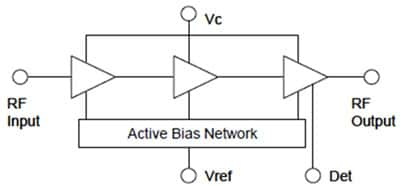
Many companies are also using InGaP/GaAs heterojunction bipolar transistors to deliver a multi-standard MMIC power amplifier for wireless network applications such as 802.11b/g/n. Examples of such amplifiers include the LX5518 and LX5516 from Microsemi. The LX5518 amplifier operates over 2.4 to 2.5 GHz and provides a power gain of 30 dB from a single positive supply voltage of 3 to 5 V. Housed in a tiny 3 x 3 mm quad flat package, the MMIC contains a three-stage amplifier architecture along with active bias, on-chip input matching and output pre-matching to simplify system implementation (Figure 2). An on-chip power detector at the output port helps reduce the system cost and circuit-board space required to implement power control in a typical wireless system. The LX5516 has a slightly simpler architecture, employing a two-stage amplifier along with on-chip active bias and 50 Ohm impedance matching on both the input and output. It has a power gain slightly less than the LX5518 and an active current of about 130 mA from a 3.3 V supply.

A similar power amplifier targeted at Bluetooth Class 1 systems, the µPG2314T5N from California Eastern Laboratories (CEL) is designed for low-power operation, drawing an active current of 65 mA when powered by a 3 V supply. This amplifier has a power-added efficiency of close to 50 percent and an output power of+20 dBm with a 3 V supply. Housed in a tiny, 1.5 x 1.5 x 0.37 mm six-contact plastic TSON (thin, small-outline non-leaded) package, the amplifier occupies minimal board space and requires few external components.
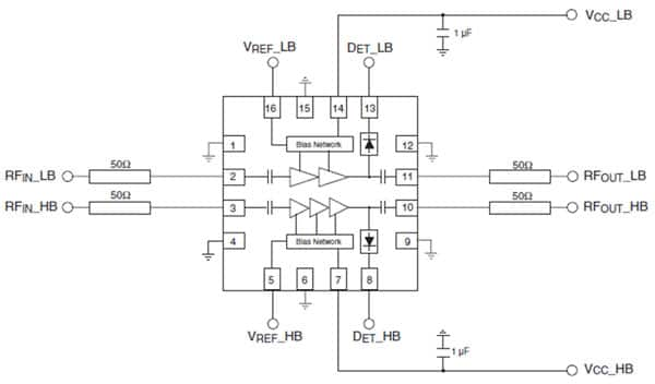
Also employing an InGaP/GaAs HBT process are the dual-band and single-band amplifiers offered by Microchip via its acquisition of Silicon Storage Technology. For example, the SST13LP05 is a dual-band power amplifier that operates in a 2.4-2.5 GHz or 4.9-5.8 GHz band, typically delivering 29 dB of gain in the lower band and 29 to 26 dB in the high band (Figure 3). Able to support applications such as IEEE 802.11a/g/b, Japanese wireless LANs, HyperLAN2, various multimedia wireless streaming applications, home RF, and cordless phones, the chip requires few external components to complete the system solution and occupies just 4 x 4 mm of board space. The chip delivers stable RF and power detector performance over a large power supply voltage range and an extremely low shut-down current of less than 2 µA.
Targeting 802.11b/g/n wireless LAN applications, the SST12LP17E (Figure 3) comes in a 2 x 2 mm eight-contact surface mount package. Also fabricated with Microchip’s GaAs HBT process, the amplifier delivers a gain of 29 dB across the 2.4 to 2.5 GHz band, and has a power-added efficiency of 28 % at a power out of 21.5 dBm for 802.11g, and 33 percent for a power out of 22.5 dBm for 802.11b. Offering a modest performance improvement over the ‘LP17E, the SST12LP08 typically delivers a gain of 30 dB with a 34 percent power-added efficiency. However, this only targeted to support 802.11b/g versions of the IEEE standard.

Pushing the shut-down current to less than 1 µA, the SST12LP15A delivers a gain of 32 dB across the 2.4-2.5 GHz band, with a power-added efficiency of about 26 percent at a power out of 24 dBm for 802.11g, and about 27 percent for a power-out of 25 dBm for 802.11b. The SST12LP14A trims the shut-down current to less than one tenth that of the LP15A, to less than 0.1 µA while reducing the operating current by about one-third. However, it gives up some of the power-added efficiency, which drops to 23 percent for a power-out of 22 dBm for 802.11g and 25 percent for a power-out of 23 dBm for 802.11b. Taking aim at the IEEE 802.11a frequency band of 4.9 to 5.8 GHz, the SST11LP12 delivers a power-added efficiency of about 17 percent at a power-out level of 23 dBm for a data rate of 6 Mbits/s. The chip offers a sub-2 µA shut down current and has an idle current of about 150 mA.
Silicon solutions catching up
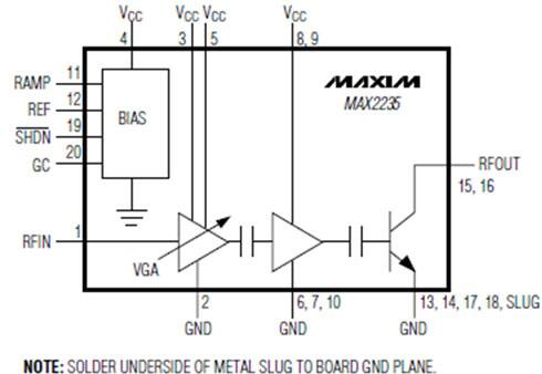
Silicon bipolar technology has been able to catch up to what was up until recently considered the exclusive domain of GaAs technology. For instance, the MAX2235, fabricated in a high-performance bipolar process by Maxim Integrated Products, targets the 900 MHz frequency band and delivers an output power of 32.5 dBm with a supply voltage of 5 V, 30 dBm at 3.6 V, 29 dBm at 3 V, and 28 dBm from a 2.7 V supply. Some of the intended applications for this PA include AMPS, two-way paging, or FSK-based communications in the 900 MHz ISM band. The chip includes an adjustable gain over a 37 dB range and has a power-control pin that adjusts the gain and bias levels to maintain optimum efficiency, even at the lower output power levels. At +30 dBm of output power, efficiency is typically 47 percent (Figure 4). When the shut-down control pin turns the PA off, the supply current drops to less than 1 µA.

Another amplifier offered by Maxim is the MAX2059, a high-linearity, digitally-controlled, variable gain amplifier that provides up to 56 dB of total gain range, with typical output IP3 and output P1 levels of 31.8 and 18.4 dBm, respectively. The chip is well suited for applications such as single and multicarrier 1,700 to 2,200 MHz DCS, 1800 PCS, 1900 EDGE, CDMA2000, WCDMA/UMTS, and TD-SCDMA base stations. A highly integrated subsystem, the chip contains two 5-bit digital attenuators, a two-stage driver amplifier, a loopback mixer, and serial interface to control the attenuators.
Targeting operation at 3 V to meet the needs of handheld systems, a silicon MMIC offered by CEL , the UPC2771TB, delivers a gain of 21 dB over the 900 to 1,500 MHz frequency band. The device’s saturated output power is 12.5 dBm at 900 MHz and 11 dBm at 1,500 MHz. The chip has a typical idle current of about 36 mA, but does not include a shut-down control capability.
Avago Technologies also offers a simple silicon bipolar Darlington amplifier targeted for operating frequencies ranging from DC to 2.5 GHz. At 900 MHz, the ADA-4643 offers a gain of 17 dB, and consumes just 35 mA from a 3.5 V supply. The chip is fabricated with the company’s HP25 silicon bipolar process that employs a double-diffused structure with self-aligned sub-micron emitter geometry, resulting in a high fT (25 GHz) and high NPN device breakdown (6 V BVCEO).
Also offering a wide range of bipolar, silicon-based amplifiers, NXP has developed MMICs such as the BGA6289 and BGA6589, wideband power amplifiers which deliver output power levels of 17 and 20 dBm, respectively. The internal gain blocks employ resistive-feedback Darlington-configured amplifiers and can operate from a typical supply voltage of 4.1 (BGA6289) or 8 V (BGA6589) while consuming about 88 or 150 mA, respectively.
Summary
The power amplifier in any wireless system typically consumes a significant amount of power when transmitting, and often continues consuming significant power as long as it on, even though it may not be transmitting any data. As we have seen, the latest generation of PAs are changing that, thanks in part to new standby capabilities that considerably reduce the standby mode power consumption, and increase transmit efficiency when the wireless system is transmitting. This article examined the latest architecture and process developments in power amplifiers that result in more-efficient and lower power systems, which, in turn, will translate into longer battery life and longer talk times between battery charges. For more information on the products mentioned, please use the links provided to access product pages on the DigiKey website.
免责声明:各个作者和/或论坛参与者在本网站发表的观点、看法和意见不代表 DigiKey 的观点、看法和意见,也不代表 DigiKey 官方政策。


