Conducted and Radiated Emissions Reduction Techniques for Power Modules
投稿人:电子产品
2011-12-27
DC/DC converters are a great high-frequency noise source. Designers must take careful steps to minimize and contain this noise near and around the converter to keep it from affecting other system components or the AC mains. We do not want our product to come back from testing and find that we have failed electromagnetic interference (EMI) or conducted emissions (CE) exams. Even more than that, we do not want these noise sources to degrade our product performance, so we need to understand the mechanisms of this noise and how to minimize it.
Radiated emissions (RE) or electromagnetic interference (EMI)
Many modules have five-sided shielding that effectively contains radiated emissions from adjacent components. Typically, the sixth side, which faces the printed circuit (PC) board, is not shielded, but it is recommended that a ground plane be placed beneath the converter and tied to the case. This method is the best means to contain the EMI emanating from the converter. Power-One power supplies, for example, have a metal-shielded construction and the company provides CE and RE data sheet curves for its CPA and CPS Series of off-board modular power solutions.
Base-plated converters will offer improved protection from near B-field radiation. At most frequencies, a base-plated converter will be approximately 10 dB/µM quieter than the open frame design.
Modular power products are typically designed to pass Comité Internationale Spécial des Perturbations Radioelectrotechnique (International Special Committee on Radio Interference, or CISPR) and Federal Communications Commission (FCC) standards. CISPR standards generally relate only to electromagnetic compatibility (EMC) emission test methods and limits.
Basic guidelines for minimizing EMI are as follows:
- Keep current loops small (Figure 1). The ability of a conductor to couple energy by induction and radiation is lowered with a smaller loop, which acts as an antenna.
- For pairs of copper printed circuit (PC) board traces, use wide (low impedance) traces aligned above and below each other.
- Locate filters at the source of interference, basically as close to the power module as possible.
- Filter component values should be chosen with consideration given to the desired frequency range of attenuation. For example, capacitors are self-resonant at a certain frequency, beyond which they look inductive. Keep bypass capacitor leads as short as possible.
- Locate components on the PC board with consideration given to proximity of noise sources to potentially susceptible circuits.

Figure 1: Avoiding large loops will minimize EMI or RE. (Courtesy of Lineage Power)
There is no single perfect EMI strategy for all applications, but some basic thought beforehand can make the task much easier. The first step is to make sure that the location of components minimizes noise. For example, decoupling capacitors should be located as close as possible to the converter, especially X and Y capacitors. Use ground planes to minimize radiated coupling, minimize the cross-sectional area of sensitive nodes, and minimize the cross-sectional area of high current nodes that may radiate such as those from common mode capacitors.
The location of the EMI components is critical; avoid placing the converter in close proximity to your filter to avoid noise coupling back into the filter. Keep in mind that you are not just filtering the power supply, but all the circuitry that the converter is powering as well. Most of today's communication cabinets employ as much local filtering as possible at the card level, and then another filter at the power entry module, where the power feeds will enter your cabinet.
CUI Inc. has its V-Infinity power module series and an excellent white paper on that series for EMC considerations in power modules.
Surface-mount modules vs. through-hole modules
Surface-mount devices (SMD) are better than leaded devices in dealing with RF energy because of the reduced inductances and closer component placements available. The latter is possible due to the reduced physical dimensions of SMDs. This is critical to two-layer board design, where maximum effectiveness from noise-control components is needed. Generally, leaded capacitors become self-resonant (become more inductive than capacitive) at about 80 MHz. Because noise above 80 MHz needs to be controlled, serious questions should be asked if a design is to be executed only with through-hole components.
Conducted emissions (CE)
Fast voltages and current changes in DC/DC converters will cause conducted noise on the input of the modular device. Fast rise-time and fall-time on logic loads will produce conducted noise that also reflects back into the input. Conducted noise will tend to generate electrical and magnetic fields that will radiate noise if circuit runs are not properly configured. Usually good layout and filter design will minimize this effect.
In order to best understand the source of CE, emissions are classified as differential (symmetrical) or common (asymmetrical) mode noise. The definition of common mode (CM) and differential mode (DM) voltages and currents is shown in Figure 2.

Figure 2: Definition of differential and common-mode currents and voltages.
EMI reduction solutions
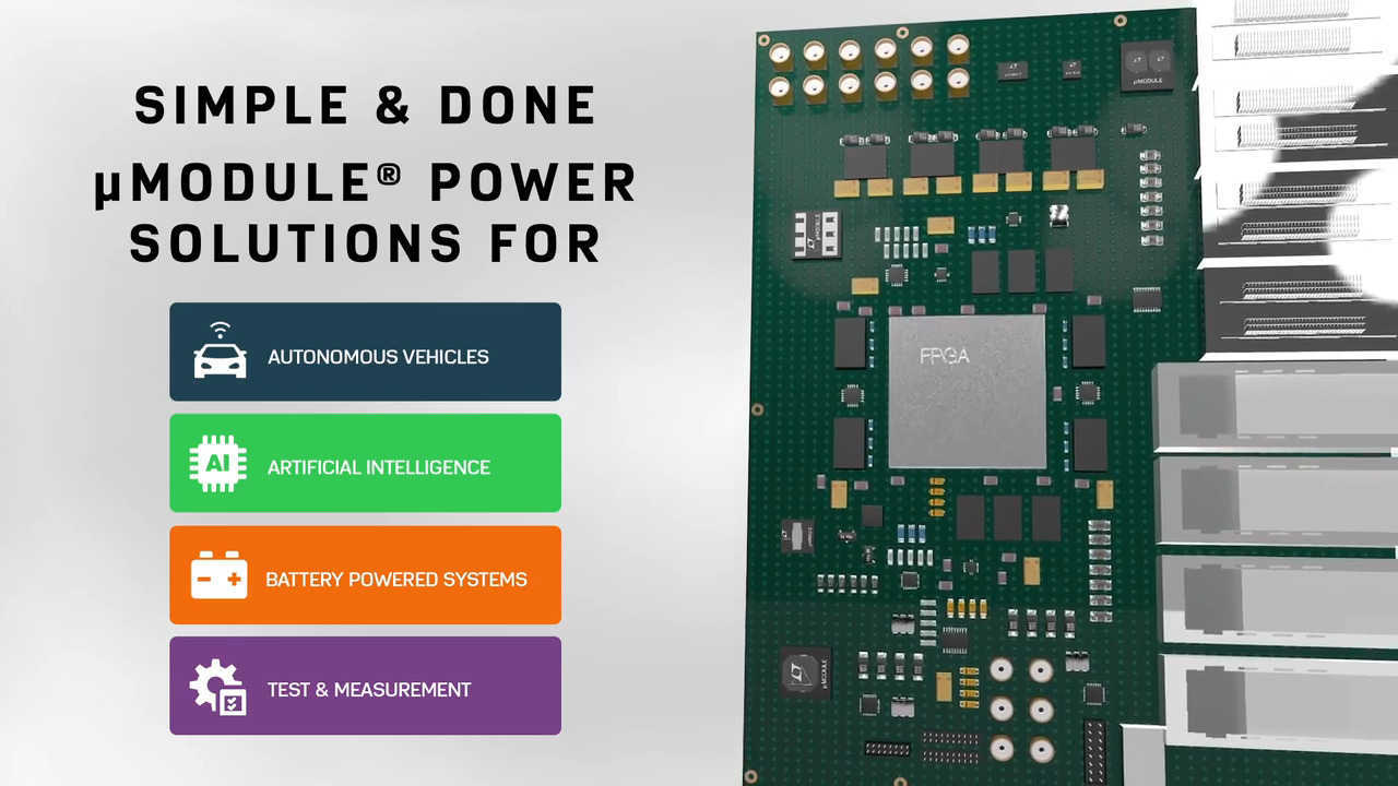
One answer is to use a pre-tested solution such as μModule regulators from Linear Technology, which are designed to bring peace-of-mind to designers by attenuating conducted and radiated energy at the source: the DC/DC regulator circuit.
Another way to minimize CE is to have voltage paths to or from the module run adjacent and parallel to each other (symmetry is always a good form of CE and EMI reduction) with a ground plane beneath. Multiple paths can be stacked on top of each other as well. This is similar to running two wires in a twisted-pair configuration that is best for cancelling common-mode noise. Avoid circuit path runs in large loops, which will act as antennas. Keep close proximity of the power conductors, which will minimize the loop area and keep RE down as well.
An external input and/or output filter may also be needed. If so, then great care must be taken to avoid undesirable effects by the stray inductance and/or capacitance of the filter, which may cause instability or performance degradation in the overall on-board power system.¹
The designer must keep in mind the impedance mismatches between the input filter and power module (Figure 3).

Figure 3: Proper impedance matching prevents undesirable effects. (Courtesy of Lineage Power)
The input of a DC/DC power module is a constant power at low frequencies. As the voltage decreases, current increases. This will present negative impedance at the input source. The converter will oscillate when the combination of the input filter’s impedance and the power module impedance becomes negative, causing a mismatch to occur. One way to prevent this is to ensure that the output impedance of the filter is much smaller than the input impedance of the power module at all frequencies. Figure 4 presents a plot of impedance vs. frequency of the input filter’s output and the power module input.

Figure 4: Stability plot for input filter/power module. (Courtesy of Lineage Power)
The output of the input filter is shown on the lower graph. At each slope change the component that contributed to that change is noted. The resonant frequency of the filter is shown as ωf. Its peak is proportional to the filters damping ratio. So an under-damped filter will most likely cause oscillations if its maximum impedance gets close to the power module impedance.
The upper curve plots the input impedance of the power module. The resonant frequency of the converters output filter is shown as ωo. Any external output filter will shift this point.
A robust and stable design combination would be to design the filter so that its peak output impedance (the resonance frequency of the filter) is one decade or more below the dip in the power module input impedance (the resonant frequency of the power module’s output filter in combination with any external output filter). It is also prudent to design the filter with a minimum damping factor of 0.707.
X and Y capacitors
X capacitors are connected between the line phases and are effective against symmetrical interference (differential mode).
Y capacitors are the EMI capacitors that are connected from the input power feeds to chassis ground and are effective against asymmetrical interference (common mode). Sometimes they are connected from each converter's power output terminal to chassis ground as well. Typical filter designs use 2,700 pF Y capacitors. The voltage rating depends on the insulation and isolation safety rating of the -48 Vdc supply. If you are unsure of these attributes, use capacitors rated to 2,000 V. If the -48 V is a reinforced insulation scheme, then 100 V-rated capacitors will suffice. An example of EMI suppression with X and Y capacitors is shown in Figure 5.

Figure 5: Example of EMI common mode and differential mode suppression with X and Y capacitors. (Courtesy of EPCOS Inc.)
EPCOS has a series of EMI suppression capacitors with the company’s model B3293X series.
Synchronization
Synchronizing power modules has the benefit of eliminating beat frequencies caused by two or more devices operating at frequencies that are close to one another. If we can operate multiple power modules at the same frequency, any EMC emissions generated will have a similar spectral density, making it easier to filter out that particular frequency. Of course, the power module must have a SYNCH pin to apply an external frequency. Some modules have access to the internal oscillator, then that oscillator can be used to drive the other modules’ SYNCH pins in a master/slave configuration.
Physical orientation
Sometimes, turning a power module and/or other magnetics 90°, such as transformers and inductors, can improve EMI performance of a power supply design. Even subtle design changes can cause a power supply to have higher EMI than necessary. Designers need to understand where noise originates and how to reduce it to acceptable levels in the particular system it will serve. This article provides some proven techniques that should make a first order improvement in troublesome EMI, which will always be a challenge to designers.
References:
- Lineage Power application note, March 2010, “Application guidelines for on-board power converters”, Sally E. Savino, Gabriel G. Suranyi.
免责声明:各个作者和/或论坛参与者在本网站发表的观点、看法和意见不代表 DigiKey 的观点、看法和意见,也不代表 DigiKey 官方政策。