High-Side MOSFET Driver
2024-03-22 | By Tobias Bruckmann
Introduction
In power electronics, the half-bridge is one of the most ubiquitous circuit parts. It can be found in a variety of power converter systems, from power supplies to motor control applications. As depicted in the schematic below, such a half-bridge consists of two transistors connected in series between the DC-Link rails.

In this case, the transistors are N-Channel MOSFETs. By forcing one of the transistors into the conducting state, the output node can be connected to one of the input potentials with low resistance. Achieving a controlled switching of the MOSFETs is done by a Gate or MOSFET driver. Its job is to charge and discharge the gate-source capacitance of the switching device to ensure a secure and timely turn on and turn off.
Motivation
Having seen the half-bridge architecture with N-Channel MOSFETs it is apparent that charging the GS-capacitance of the low side MOSFET will be the easier task since its source potential is fixed to GND. While there are still a variety of Gate-Driver architectures to choose from, they all operate by charging the GS-capacitance from a voltage or current source with reference to GND. One easy example architecture is shown below.

The complication with switching the high-side transistor lies in the fluctuating nature of its source potential. Due to this complication, charging its GS-capacitance from a simple ground-referred voltage source becomes problematic. There are crude ways to achieve high-side control with ground-referred voltage inputs, but they come with substantial drawbacks. One approach would be to use a voltage higher than VDCLink, one P- and one N-Channel MOSFET as well as a Zener-Diode and a protective resistor as shown below.

The drawbacks of this approach are obvious. Not only will the Zener-Diode waste a lot of power. Its thermal limits and efficiency considerations thereby limit the maximum gate current and slow down the switch-on transients. It should also be noted that the depicted approach will fail to safely turn on the MOSFET in case VOUT exceeds VDCLink due to external influences. As we have seen a P-Channel MOSFET seamlessly being operated in high-side switching above, choosing this semiconductor type as a high-side power switch might seem like an easy solution. But most of the time it is not. Due to the semiconductor physics underlying N- and P-Channel MOSFET operation, they are no match in power capabilities when compared in equal size and price categories. It is due to the P-Channel´s lower specific conductivity that finding a power device of this type is commonly not possible.
Solutions
Considering the need for half-bridges in power electronics and the physical limitations of P-Channel devices, different solutions for driving high-side N-MOS power transistors have been developed. One of them is shown below.

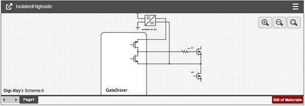
The depicted so-called Bootstrap concept relies on a capacitor to supply the needed charge for switching the power semiconductor. It’s like going up a mountain and passing a stream with an empty water bottle. You know you will be thirsty once at the summit, and it’s also apparent that there will be no water to fill your bottle up there. So, you store some now and take it with you. That’s exactly what C1 does. When the output potential is low, C1 is being charged through D1, storing charge, and creating a potential difference between the poles of C1. Ignoring parasitic effects, this potential difference remains even when VOUT rises. D1 will block as soon as VC1 + VOUT exceed VIN keeping C1 charged. With adequate dimensioning of all components and given that VOUT assumes small values for enough time to charge the bootstrap capacitor during each cycle, this concept can provide the needed supply voltage for high-side switching. But parasitic effects leading to undesired discharge of C1 and the need for a minimum output low time for recharging limit the applications of this architecture. With great respect for all other driver architectures, the next solution was chosen due to its wide range of applications. This approach can be simplified as the following: You need an isolated voltage source, so you use one. Instead of using a stored fixed amount of charge, the auxiliary voltage is created using a transformer. This way it is free of any reference due to the galvanic isolation and can be attached to the source potential of the high-side switch, ensuring a fixed supply voltage analog to the environment of low-side drivers. This concept is schematically shown below.

Usually, the isolated voltage converter is implemented in a flyback topology. It is here that the water analogy breaks down. Using a flyback converter to create the auxiliary voltage is like having a water wheel at a fixed position in a stream, that through some kind of coupling moves water from wherever your feet are to wherever your mouth is at. And although this does not make any intuitive sense, we may still appreciate the Electronic-hydraulic analogy despite its shortcomings. Explaining the inner workings of a flyback converter will be the topic of another blog post.
Have questions or comments? Continue the conversation on TechForum, DigiKey's online community and technical resource.


