


Design Transimpedance Amplifiers for Precision Opto-Sensing
投稿人:DigiKey 北美编辑
2017-07-13
Photodiodes and their associated transimpedance or pre-amplifiers are the bridge between light and a useful output voltage. Though they are fundamental elements, designing the circuitry necessary for precision instruments presents a multi-dimensional set of problems and requires particular attention to parameters, such as phase margin.
The phase margin is particularly critical as it determines the circuit’s step response, overshoot characteristics, and quality factor (Q). However, getting to the required phase margin is a process.
At the start of the transimpedance amplifier (TIA) design, the designer defines the operational amplifier’s (op amp) output swing. From that point, the designer proceeds to define the feedback resistor and capacitor, which determines the TIA’s phase margin.
This article will briefly discuss the op amp’s usable output swing range, followed by the target phase margin derivations.
The use of TIAs in photo sensing circuits
Photo sensing circuits such as transimpedance amplifiers (TIAs) are useful in precision systems such as computed tomography (CT) scanners, blood analyzers, and smoke detectors. Other uses for light-to-voltage conversions are with position sensors, infrared (IR) pyrometers, and chromatographs. In these circuits, photodiodes generate a small current, which is proportional to the level of illumination.
The TIA converts the photodiode’s current output signal to a usable voltage level. The implementation of this current-to-voltage conversion consists of a photodiode, an amplifier and a resistor/capacitor feedback pair (Figure 1).

Figure 1: Zero reverse bias TIA circuit with a photodiode and amplifier in simplified mode. This TIA circuit contains the parasitic amplifier input capacitances as well as the photodiode junction capacitance. (Image source: Digi-Key Electronics)
Surprisingly, this application circuit presents a large multi-dimensional set of problems, the most challenging of which is meeting the preferred phase margin. For designers to get it right, they must use the circuit’s phase response to determine the circuit’s step response, overshoot characteristics, and Q factor.
Defining the feedback resistor, RF
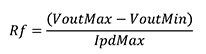
The phase margin is a function of the feedback resistor and capacitor in the feedback loop, so the first task is to define the feedback resistor. The value of the feedback resistor, RF, depends upon the maximum photodiode current (IPDMAX) and the output voltage range of the op amp. As mentioned earlier, the application environment defines IPDMAX.
The photodiode model contains an ideal diode (DPD) and the photodiode light-excited current source (IPD) (Figure 1, again). The current range of IPD is zero amperes to IPDMAX. The user determines the value of IPDMAXto be equal to the maximum photodiode current in accordance with the maximum light brightness.
The notation for the minimum and maximum voltage values are VOUTMIN and VOUTMAX, inclusive. In this configuration, the determination of the VOUTMIN limit is equal to the greater of the Iin+ input negative common-mode voltage or the amplifier’s minimum linear output. In this circuit, VREF provides the VOUTMIN value.
The amplifier’s maximum linear output determines the VOUTMAX limit. The datasheet’s open-loop gain test conditions define the widest values for the linear range of VOUTMIN and VOUTMAX.
The final values for IPDMAX, VOUTMIN, and VOUTMAX define the RF value (Equation 1).
Design in the preferred stability
In a previous article, “How to Design Stable Transimpedance Amplifiers for Automotive and Medical Systems”, we used three simple formulas to quickly provide a working circuit with a 45-degree phase margin. A circuit with a 45-degree phase margin will produce 23% overshoot from a step response (Figure 2).

Figure 2: This is an ideal, normalized step response of a TIA with a 45-degree phase margin. (Image source: Texas Instruments)
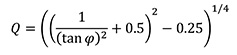
In this figure, the normalized signal produces a peak of 1.23 V, which indicates an overshoot value of 0.23 V or 23%. To take this further, the circuit quality factor (Q) is approximately 1.19 (Equation 2). In this equation, j is the phase margin.
The graphical representation of an ideal step response shows the overshoot of the TIA circuit (Figure 2).
The graph in this figure shows a normalized step response output. This system is normalized to 1 V. The overshoot percentage is equal to the peak signal value minus one.
A 45-degree phase margin may be undesirable for many designs. The poles and zeros in the TIA design control the assignment of the phase margin, and hence the overshoot. The various poles and zeros in the TIA circuit can be manipulated by simply adjusting the feedback capacitor, CF.
Calculating the TIA’s design frequencies
A Bode plot of the elements in the TIA circuit is useful in this discussion. This Bode plot contains the response of the amplifier and the response of the closed-loop noise gain (Figure 3).

Figure 3: The Bode plot of the amplifier’s open-loop curve (red) superimposed on the TIA noise gain curve (blue). (Image source: Digi-Key Electronics).
The construction of the amplifier must incorporate a voltage feedback topology. The significant amplifier frequencies in this Bode plot are fAOL and f3dB. The lowest frequency, fAOL, represents the dominant pole in the amplifier’s open-loop gain curve (Equation 3).
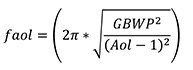
Where GBWP = amplifier gain bandwidth product and AOL = amplifier open-loop gain in volts/volts units.
The second amplifier frequency, f3dB, is the maximum stable bandwidth of the amplifier times the tangent of 60 degrees (Equation 4).
![]()
Where GBWP = amplifier gain-bandwidth product and AVClMin = amplifier minimum stable closed-loop gain
This equation assumes that the amplifier designer created the amplifier with a 60-degree phase margin for the maximum stable bandwidth of the amplifier. This assumption is conservative and one can make adjustments in accordance with the selected amplifier.
The three noise gain frequencies of interest in the TIA circuit are fZ, fP and fI. Calculate the transfer function of the noise gain at the non-inverting input of the amplifier (Equation 5).
![]()
Where CIN = CPD + CCM + CDIFF (per Figure 1)
The lowest frequency, fZ, is the first and only zero in the noise gain transfer curve (Equation 6). This frequency is dependent on all resistors and capacitors in the circuit.
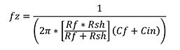
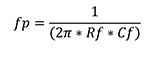
The middle frequency, fP, is the first of two poles in the noise gain system. This frequency is dependent on the feedback system containing RF and CF (Equation 7).
![]()
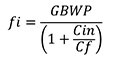
The higher noise gain system frequency occurs where the amplifier’s open-loop gain intersects the closed-loop noise gain curve, fI (Equation 8).
Calculating the TIA’s phase margin
To determine the phase margin of the system, start by selecting a feedback capacitor and comparing the distance of each frequency to the frequency where the open-loop gain of the amplifier intersects with the noise gain curve, or fI. In this manner, each pole and zero in the system contributes to the circuit’s total phase margin.
For instance, the contribution to phase shift of the noise gain pole (fP) is the inverse tangent of fI divided by fP or arctan (fI/fP). The TIA phase margin calculation includes all the frequencies that we have discussed (Equation 9).

Putting theory into practice
To find the value of the feedback capacitor (CF), the process is a follows:
- Select the amplifier/photodiode
- Determine the maximum photodiode current
- Calculate RF, by selecting the amplifier’s output swing voltages
- Calculate CF through iteration
Selecting the amplifier: The input bias current and input offset voltage must be low. If the input bias current is high it will compete with the photodiode current signal. It is preferable that the room temperature amplifier input bias current is less than a few hundred picoamps (pA). Remember, in relation to the photodiode, this current will generate DC errors. Additionally, the amplifier’s input offset voltage must be low, preferably less than 0.1 mV. Higher offset voltages create a linearity problem with the photodiode.
The Texas Instruments OPA192IDBVR meets these specification limits, with an input bias current and input offset voltage of +/-20 pA (max) and +/-25 microvolts (µV) (max), respectively.
Here’s some additional important datasheet information about the OPA192IDBVR (for VS = +/-5 V)
- Unity-gain stable: AVClMin = 1 V/V
- Gain-bandwidth product: GBWP = 10 MHz
- DC Open-loop gain: AOL = 134 dB = 5.012 M V/V
- Common-mode voltage range: -5.1 V to 5.1 V
- Open-loop gain test conditions: -4.4 V to 4.4 V
- CDIFF = 1.6 pF
- CCM = 6.4 pF
Selecting the photodiode: The Vishay Semiconductor, Opto Division’s TEMD6200FX01 is an ambient light sensor PIN photodiode. This device is suitable for applications that require wavelength sensing of 540 nanometers (nm) (typ). The junction capacitance of this device is 60 picofarads (pF). In our application IPDMAX will be 10 µA.
Calculating RF: We will use an output swing of +/-4 V. This output swing is within the limits of the OPA192IDBVR’s input common-mode voltage range and the linear output voltage range. Using Equation 1, RF = 800 k Ohm (kΩ).
Calculating CF: At this point we have all the formulas we need to achieve a 65-degree phase margin. A definitive formula to find the value of CF for a random phase margin does not exist. As a first estimate, we will select a signal bandwidth for the TIA of GBWP/100 and then apply Equation 9 to get the phase margin. The signal bandwidth is equal to fP.
Various phase margin calculations identify the proper value for CF (Table 1).
|
||||||||||||||||||||||||||||||||||||||||
Table 1: Calculated feedback capacitor (CF) versus phase margin using OPA192IDBVR and TEMD6200FX01 in a TIA circuit. (Image source: Digi-Key Electronics)
The TIA is a second-order system. The OPA192IDBVR and TEMD6200FX01 combination in a TIA requires a CF of 1.757 pF to achieve a phase margin of 65.6 degrees. For a second-order system and the TIA, a 65.6-degree phase margin and Q of 0.706 resembles a Butterworth filter response.
Conclusion
This article provides appropriate design equations to obtain a desired TIA phase margin. The required parameters for an op amp in the TIA circuit are input bias current equal to or below 100 pA, input offset voltage equal to or less than 0.1 mV, as well as a voltage feedback topology. It is possible to design a TIA with a preferred phase margin through calculation iteration. Review and understand the design formulas to successfully design a custom TIA circuit.
References
- Graeme, Jerald, Photodiode Amplifiers: Op Amp Solutions: McGraw-Hill, 1996, ISBN: 0-07-024247-X
免责声明:各个作者和/或论坛参与者在本网站发表的观点、看法和意见不代表 DigiKey 的观点、看法和意见,也不代表 DigiKey 官方政策。


