


Right-Sizing Your Wireless Design for Power and Cost
投稿人:Convergence Promotions LLC
2011-08-08
Wireless solutions are popping up everywhere, but in the case of portable consumer devices in particular, power consumption and cost represent some serious constraints.
Designing with RF is no longer the mysterious and difficult challenge it used to be. Advances in process technology, coupled with the availability of system-on-chip (SoC) architectures, have brought the price of RF down while significantly simplifying design. As a result, wireless technology is being integrated into nearly every type of application, including healthcare equipment, lighting control, security, energy management, gaming, and many other embedded and industrial applications.
Often, the application defines the topology, protocol, and RF technology that will be required. For example, a wireless heart monitor would likely use a point-to-point topology. If the monitor needs to speak to a conventional network, ZigBee® may be the best protocol to use. However, if the monitor is paired to a specific piece of exercise equipment, a proprietary protocol utilizing a sub-GHz radio may be appropriate and more cost-effective. In many cases, the primary design challenge remaining is selecting the implementation that provides the performance required while minimizing cost and power use.
The system-on-chip approach
Today's SoC architectures are able to combine an RF radio with an MCU with sufficient processing capacity to handle the appropriate protocol stack and still have enough headroom to run an application (see Figure 1). Texas Instruments (TI), for example, offers SoCs which support nearly every wireless technology available, including:
CC2530: ZigBee plus 8051 MCU
CC2560: Bluetooth® plus MSP430 controller
CC2540: Bluetooth Low Energy plus 8051 MCU
CC430: Sub-GHz radio plus MSP430 controller

Figure 1: The TI CC430 combines an RF radio with an MCU. (Source: Texas Instruments. Used with permission.)
With an SoC, an entire RF application can be implemented with a single processor. To accommodate the different requirements of each protocol and application, each SoC family offers products with varying degrees of integration so that developers can select a device optimized for their particular system. With several choices of processor speed and memory depth, developers have the option of supporting advanced features such as security or hub/mesh capabilities. Many devices offer optional analog peripherals, enabling the SoC to integrate sensor functionality to handle low frequency tasks such as monitoring a system's temperature, up to high frequency sensing such as is required to manage a capacitive touch screen. A variety of interfaces may also be available, including USB, so that these SoCs can communicate with other system components. Some devices even integrate an LCD driver to enable single-chip design of portable devices such as glucometers.
Many SoCs have features which allow developers to add advanced features and, as a consequence, significant value to devices. In addition, these SoCs have already been optimized for performance and power efficiency. Designing around an SoC architecture simplifies RF design to the point of enabling engineers with little to no RF experience to introduce wireless capabilities into a system. It provides a production-ready subsystem that significantly reduces time-to-market. In many cases, especially when a company does not have RF expertise in-house, an SoC can come at a lower total cost of ownership when factors such as hardware and software development costs, along with time-to-market delays, are already addressed.
TI also provides a variety of resources to accelerate RF design. Its SmartRF® Studio, for example, enables developers to easily change radio settings such as sensitivity and output power to facilitate system optimization (see Figure 2). With a wide range of application-specific development kits — including the RF2560 EZ 430 Bluetooth EVM and Chronos wireless development kit with a wristwatch form factor [1] — developers can assess different wireless technologies in less than a few hours. In addition, pads or pins on the EVMs allow for real-time power measurements to enable accurate profiling of power consumption.

Figure 2: SmartRF® Studio from TI. (Source: Texas Instruments. Used with permission.)
TI also offers radio-only transceivers which connect to an external processor via a standard embedded interface. If a system is extremely simple and does not require an LCD or ADC, a transceiver interfaced to a small MCU will be the most cost-effective approach. However, many of today's embedded and medical applications require a high level of intelligence, and this approach would require developers to perform much of the heavy lifting behind RF design.
STMicroelectronics' approach to wireless is its STM32W SoC processor which integrates an IEEE 802.15.4 WPAN™-based 2.4 GHz radio with a Cortex™-M3 processor. Also a single-chip implementation, the STM32W offers 128 K of code space, providing ample room for a ZigBee protocol stack and full application. The STM32W offers several low-power modes (see Table 1) and integrates a variety of features that together increase the power efficiency of wireless applications:
| Built-In Voltage Regulator: This allows the STM32W to run off of a single lithium coin cell battery. |
| Dynamic Voltage Regulation: The system can be disconnected from power, leaving only the clock functioning with wake-up capabilities. |
| Programmable Frequency: The STM32W can be clocked slower to conserve power. |
| Full Peripheral Control: Each peripheral can be turned off when it is not being used. |
| RAM Retention: When a processor goes to deep sleep, RAM must first be saved in non-volatile memory. This can create issues, such as startup latency as a system reloads the LCD display memory or needs to read a sensor. The STM32W offers a low-power mode that retains RAM, enabling fast wake-up responsiveness. |
| Mode | Regulators | Low-frequency 10 kHz RC oscillator | 32 kHz crystal oscillator | High-frequency 12 MHz RC oscillator | 24 MHz crystal oscillator | Power consumption |
|---|---|---|---|---|---|---|
| Deep sleep 2 | off | off | off | off | off | 0.4 μA |
| Deep sleep 1 | off | on | optional | off | off | 0.7 μA |
| Standby | on | on | optional | off | off | 2 mA |
| Active at 12 MHz | on | on | optional | off | on | 6 mA |
| Active Mode | Sensitivity | Rx current | Tx current | Tx current |
|---|---|---|---|---|
| Radio Peripheral | dBm | mA | mA at 0 dBm | mA at -32 d Bm |
| -100 | 20 | 24 | 15 |
Table 1: The STM32W low-power modes. (Source: STMicroelectronics. Used with permission.)
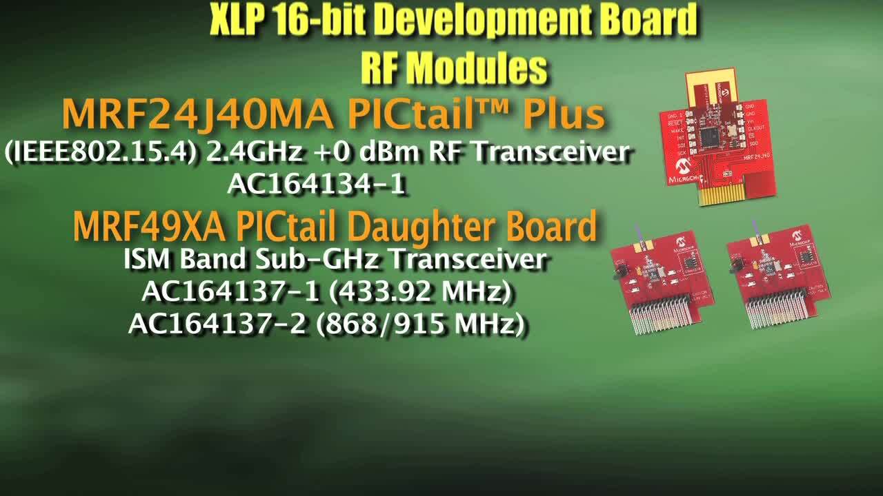
Taking a modular approachOffering an even higher level of integration are RF modules. Microchip's approach to RF, for example, is to offer PCB-based modules supporting different RF technologies ranging from 2.4 GHz to sub-GHz frequencies that provide the entire RF subsystem except for the MCU (see Table 2).
IEEE 802.15.4 Transceivers/Modules
| Device | Pin count | Freq Range | Sensitivity | Power output | RSSI | Tx power | Rx power | Clock | Sleep | MAC | MAC feature | Encryption | Interface | Package |
|---|---|---|---|---|---|---|---|---|---|---|---|---|---|---|
| MRF24J40 | 40 | 2.405 - 2.48 | -95 | 0 | yes | 23 | 19 | yes | yes | yes | CSMA-CA | AES128 | 4-wire SPI | 40-QFN |
| MRF24J40MA | 12 | 2.405 - 2.48 | -95 | 0 | yes | 23 | 19 | yes | yes | yes | CSMA-CA | AES128 | 4-wire SPI | 12/Module |
| MRF24J40MB | 12 | 2.405 - 2.475 | -102 | 20 | yes | 130 | 25 | yes | yes | yes | CSMA-CA | AES128 | 4-wire SPI | 12/Module |
Sub-GHz Transceivers/Modules
| Device | Pin count | Freq Range | Sensitivity | Power output | RSSI | Tx power | Rx power | Clock | Sleep | Interface | Package |
|---|---|---|---|---|---|---|---|---|---|---|---|
| MRF49XA | 16 | 433/868/915 | -110 | 7 | yes | 15 mA @ 0 dBm | 11 | 10 MHz | yes | 4-wire SPI | 16-TSSOP |
| MRF89XAM8A | 12 | 868 | -113 | 12.5 | yes | 25 mA @ 10 dBm | 3 | 12.8 MHz | yes | 4-wire SPI | 12/Module |
IEEE 802.11 Module
| Device | Pin count | Freq Range | Sensitivity | Power output | RSSI | Tx power | Rx power | Clock | Sleep | MAC | MAC feature | Encryption | Interface | Package |
|---|---|---|---|---|---|---|---|---|---|---|---|---|---|---|
| MRF24WB0MB | 36 | 2.412 - 2.484 | -91 | 10 | yes | 156 | 85 | 25 MHz | 0.1 | yes | 802.11 | WPA, WPA-2, WEP | 4-wire SPI | 36/Module |
Table 2: Microchip RF modules. (Source: Microchip Technology. Used with permission.)
The MCU implements the protocol stack — i.e., Wi-Fi®, ZigBee, Bluetooth, and Microchip’s proprietary MiWi™ — and connects to the radio with SPI. Depending upon the technology, base modules cost between $10 and $20 and have a small form factor of roughly 1" x 1" (see Figure 3).

Figure 3: The MRF24J40MA RF module (a) is a 2.4 GHz module that has already been certified by the FCC while the MRF24WB0MB RF module (b) provides Wi-Fi connectivity. (Source: Microchip Technology. Used with permission.)
The advantage of this approach, compared to placing the MCU on the module, is that developers can select any of Microchip's 700+ PIC® MCUs, giving full flexibility in terms of performance, memory, and peripheral options. Devices range from simple 8-bit MCUs to 32-bit MCUs which can run a wireless protocol stack, application, and high-speed interface like USB. Advanced features, such as capacitive sensing, can be added to existing designs by upgrading the MCU.
Since the protocol stacks are implemented in C, developers can transparently migrate between MCU architectures without having to rewrite applications. This allows the MCU to be the right size for each application, as well as providing a platform upon which a full line of products can be based using a single code base. Developers can also easily change RF technologies, such as offering proprietary and ZigBee-based devices, to address the requirements of specific markets with minimal code changes.
For applications in which a proprietary protocol can be used to reduce product cost, Microchip offers its MiWi protocol and development tools. Because MiWi offers a common API, developers can switch between wireless technologies without code modification. In addition, no product-level certification is required. Several of the 2.4 GHz and sub-GHz modules are footprint compatible to simplify hardware migration as well.
Modules also accelerate initial product development. Rather than working with an EVM and having to develop hardware in parallel to software, developers are able to work with the final production hardware from the start, even if they have no RF experience. Modules also serve well in applications where there is an ASIC or host processor. Rather than burden the system with TCP/IP processing, RF capabilities can be easily added by using the interface the PIC plus RF module to the ASIC/host via a UART or SPI channel.
In terms of system cost and power, the more design a manufacturer takes on internally, the more efficient the RF system can be because each component can be optimized to the application. SoCs do add some inefficiency due to the fact that RF and analog circuitry are implemented more efficiently in different process technologies. Specifically, when an MCU is implemented on the same die as an RF subsystem, this increases the cost of the MCU. Designing with an SoC, however, eliminates many RF design concerns that would challenge engineers and delay a product's launch.
The same logic applies to going with an RF module. Modules reduce RF design headaches down to a matter of connecting an MCU to a standard interface port. The cost is a little higher than it would be for a design based on an SoC, but there is very little thinking required.
It is important to note that deciding whether to use a module, SoC, or design your own RF subsystem is not as simple as it used to be. A decade ago, the breakeven point for using a module was five thousand units/year or less. If your volumes were any higher, it made sense to build your own. Today, however, advances in technology and manufacturing efficiencies have changed this number significantly. Microchip, for example, estimates that the make-your-own breakeven point for its modules approaches one hundred thousand units. Again, more than just the bill-of-materials cost of the module has to be taken into account. The RF design of a module is field-proven and all agency certifications are complete (although individual product certification, such as is required for Wi-Fi, may still be necessary). For many manufacturers, the ability to outsource this part of the production chain reduces risk and investment.
Power optimization
The key to power efficiency in RF systems is to limit, in this order, scan time, transmit time, and receive time. Scan time refers to when a device listens across the spectrum to discover if another device is trying to communicate with it. As the device must listen over every available channel, it consumes more power than when it is actually communicating. With Wi-Fi, for instance, this difference needs to be considered when evaluating whether to put the RF system into sleep or hibernate mode between transmissions. Hibernate mode enables a system to run at leakage current levels, but the device must reestablish a link with the access point when it wakes, requiring extra time and power compared to the fast wake up ability of sleep mode.
For all these modes, power efficiency is a factor of time; the less time the radio is active, the better.
Collecting data and burst transmitting is preferred, as one long transmission is better than many short ones. Also, the footprint and efficiency of the stack will come into play, since the faster the MCU can turn on, stabilize, transmit, and go back to sleep, the more power efficient the system.
After minimizing radio time, wireless systems are designed to maximize sleep time. This means that the MCU's power consumption, both in sleep and while active, can represent a significant portion of the total power consumption. The ability to right-size the processor to match the radio and application, as well as have full control over which peripherals are powered up, can be the difference between months and years of operation for battery-operated devices like glucometers and heart monitors.
Using a SoC approach also improves power efficiency since data does not need to be transmitted over an external interface between the transceiver and processor. Rather, it can be sent straight to memory. This reduces latency, which enables the system to go back to sleep sooner, and further reduces power consumption.
The integrated aspect is also important for applications such as medical equipment where reliability is important. RF can be challenging to design, and integration reduces the number of components, as well as points of failure.
Many RF systems need to wake for system events such as a key press. Ideally, the system is set to wake on an interrupt that is triggered when a GPIO pin is turned on. The number of pins dedicated to this task can be reduced to one by multiplexing several GPIO into one signal. This is a power-efficient approach to monitoring a capacitive sensor touch screen, for example.
RFID: An attractive alternative
One of the keys to reducing power consumption is to eliminate or power down circuitry a system is not currently using. Given that the wireless transceiver is one of the major power consumers in a system, significant improvements in battery operating life can be achieved by limiting transmit and receive time. However, even more substantial gains can be achieved by eliminating the wireless transceiver altogether using RFID technology.
For many medical and embedded applications, the value a wireless interface brings to the system is the ability to transmit data to a centralized location where it is processed and correlated with data from other devices. This is especially true for sensor-based applications. The transceiver enables the sensor node to receive a request for data and then transmit the data. From a power standpoint, such a system needs to continuously scan the spectrum for a request. This, for many systems, is the activity that single-handedly consumes the most power.

Figure 4: ST's M24LR64 dual-interface EEPROM has an RFID interface on one side of the chip and an I²C interface on the other. (Source: STMicroelectronics. Used with permission.)
RFID technology provides a mechanism for reducing power consumption for the wireless link to zero by eliminating the transceiver altogether. For example, the M24LR64 from ST is a dual-interface EEPROM with an RFID interface on one side of the chip and an I²C interface on the other (see Figure 4). The MCU controlling the sensor node stores data in the dual-interface EEPROM. When a user wants to collect and analyze the data, an RF reader powers the RFID interface and reads off the data without requiring any power from the sensor node's battery. Because the device is an EEPROM, no power is required to hold the data over long periods. The only time power required from the battery is to write sensor data that has just been collected. In fact, data can be read from a device even when it is turned off. The M24LR64 has a 64-Kbit capacity, supports password security (see Figure 5).

Figure 5: The M24LR64 has a 64 Kbit capacity, supports password security. (Source: STMicroelectronics. Used with permission.)
Consider a pedometer embedded in a shoe based on RFID technology. The pedometer captures movement data and records it for later collection. The complexity of this system lies not in the capture of data, but in how the data is interpreted. When data interpretation is implemented in the collector rather than the node, evolution of analysis algorithms does not require any modification of nodes; the actual process of measuring impact in the shoe stays the same regardless of how the data is used. Code upgrading is therefore unnecessary, eliminating one of the key reasons for implementing receive capabilities in a node. This results in lower node complexity and cost, which is especially important for multi-node systems (e.g., a person wears two shoes). In addition, because the cost per node is so low compared to a wireless transceiver, both in terms of dollars and power, more nodes can be introduced to a system to provide more accurate and reliable coverage.
Since the RFID cannot receive transmissions, it needs to be able to collect data in a way that always makes data available. The sensor node, each shoe in this case, collects data and stores it in a circular list that overwrites the oldest data entry. The use of timestamps enables the data collection device to determine what data has been added since the last the time the device was read. However, if the time between data collections is too long, data may be lost. This may not be an issue for systems in which data becomes too old to be useful anyway. Alternatively, the sensor node can employ techniques that compress data to enable longer periods of time between reads. For example, rather than record the temperature every second (60 samples per minute), only the highest and lowest temperature during the past minute are stored (2 samples per minute), resulting in a reading frequency 30 times longer.
With RFID technology, a device does not need to scan, transmit, or receive, thereby eliminating the major power factors of an RF subsystem. As RF is a primary source of battery drain, this approach can extend the operating life of a battery-based system significantly. Finally, RFID technology deployment in the past was limited by the ability of applications to absorb the high cost of an RFID reader. However, as reader technology continues to enter mainstream applications — for example, the new Google Nexus S cell phone has an embedded RFID reader — the volumes are increasing and leading to lower cost.
With the availability of modules and SoCs, RF has become a component like any other that can be added to a system. The actual RF signal chain can be transparent to developers, making the most difficult design decision how to size the power consumption and data rate of the RF subsystem to the actual use cases of an application. Introducing RF to a system is not yet quite as simple as adding an antenna and reading data off a SPI port. Developers still need to understand the limitations of the particular implementation they choose. They also have to know enough about how to implement the RF link to manage power consumption. However, with the tremendous number of SoC and modular choices, as well as the availability of alternative technologies like RFID, RF capabilities can be added in a cost-effective manner to nearly every type of system.
免责声明:各个作者和/或论坛参与者在本网站发表的观点、看法和意见不代表 DigiKey 的观点、看法和意见,也不代表 DigiKey 官方政策。


 中国
中国