


RF Switches Add Flexibility
投稿人:电子产品
2013-01-31
Standard mechanical switches do not work well with RF. At high frequencies, signal coupling can occur across mechanical contact gaps, which can act like a capacitor in a high-pass filter. Longer gaps reduce coupling, but impose size issues.
Semiconductor RF switches are a class of ICs that pass a desired band when active, and severely attenuate it when inactive. Mutually exclusive cascaded switches allow RF signal path multiplexing, which, in turn, allows modern equipment to share antennas or route RF to different stages.
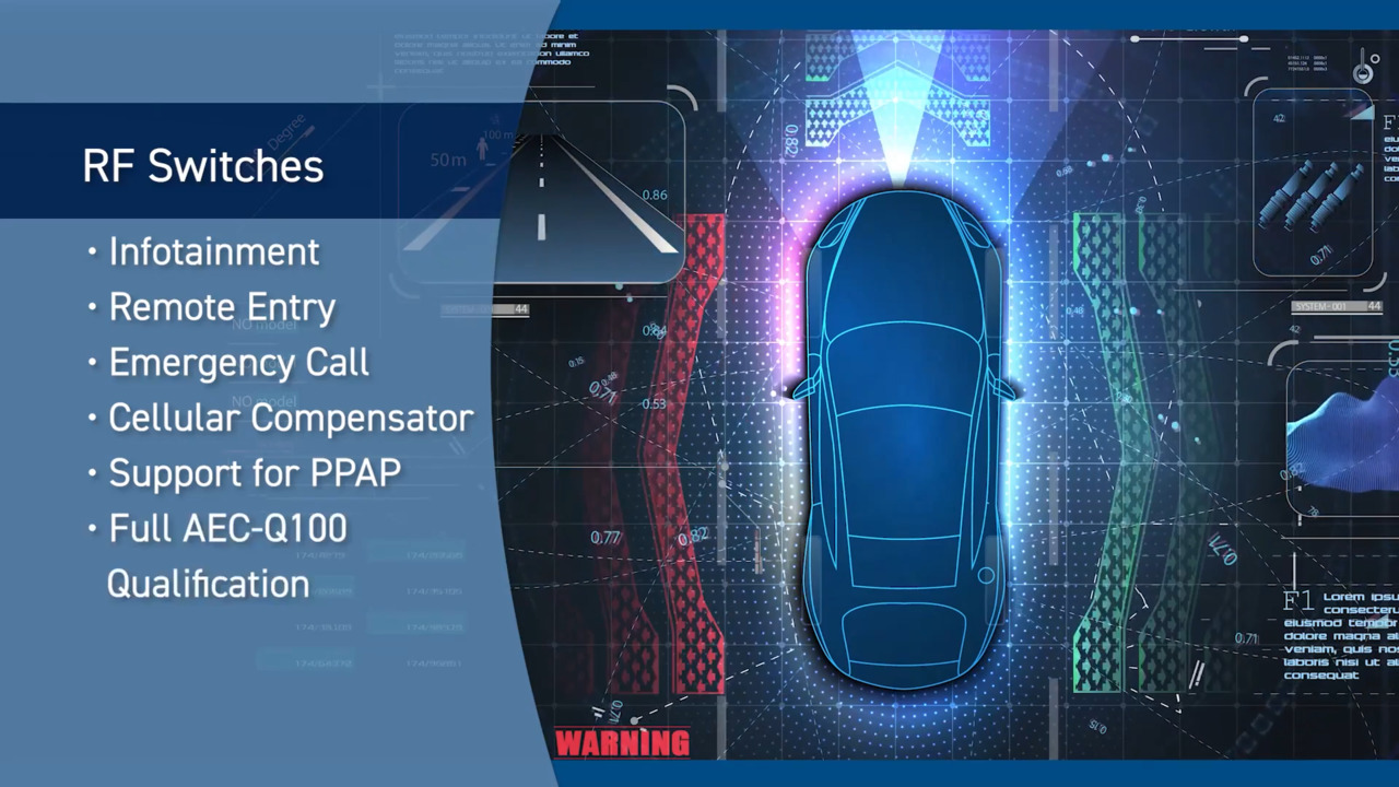
In addition, the ability to use an onboard PCB antenna or an external antenna requires switching between the two on the same board. An RF switch adds the flexibility of having one board that supports both.
This article looks at RF switch technologies and parts that are available for engineers engaging in multifunction RF designs such as Bluetooth and Wi-Fi. It will discuss size, power, and packaging options, as well as the constraints offered by presently available products. All parts, data sheets, training, and development kits mentioned are available online at DigiKey’s website.
Pin diode switches
Semiconductor switches for RF low power applications are widely used and a well understood technology. It is important to note the low power caveat, as high power switches will use specialty materials. Older ham radios, for example, still use mercury switches, admittedly not the most environmentally friendly material, but very effective at switching high power and completely safe when used properly.
For the vast majority of designs, power levels are in the range of micro-Watts to Watts, meaning semiconductor technology can easily perform well here – and it does. Two main technologies used for RF switching are PIN diode and transistor-based RF switches.
The PIN diode switch takes advantage of a ‘near intrinsic’ (lightly doped) semiconductor layer between highly doped P and N type semiconductor junctions (Figure 1). The high doping preserves low Ohmic resistance, since these are contact points for the switch.

Figure 1: PIN diodes act as switches because of high-level injection. This floods the n and p regions until the charge carrier density passes a threshold level, allowing it to conduct.
As a diode, it is normally in the off state and is non-conductive. The PIN diode is forward biased when then P and N regions are charged (potential difference is high enough) and high-level injection takes place. This is an instance where the diode is ‘flooded’ with electrons and holes, to the point where it acts as a nearly perfect linear resistor. As a result, a PIN diode forward biased acts like a variable resistor, and that is how it can be used as a switch. Achievable ranges from .1 Ohm to 10 K-Ohm have been shown, but the usable range is smaller, as we will shortly see.
A nice thing about PIN diode types of RF switches is that you can make your own if you need specialized or non-standardized characteristics. Over half a dozen suppliers provide discrete PIN Diodes with voltages up to 250 V and currents up to 1.5 A. The DigiKey parametric search engine is a useful tool for finding exactly what you need.
A typical example is the NXP BAP65-02,115, a 30 V, 100 mA device in an SOD-523 or SC-79 package. A multipart training tutorial from NXP on RF Small Signal Devices is available on DigiKey’s website.
General purpose integrated PIN diode switch devices are also available with good specifications. For example, a general-purpose part like the Skywork’s SKY12207-306LF SPDT RF switch not only handles 900 MHz to 4 GHz with a 0.4 dB insertion loss, its small 4 x 4 mm QFN package switches and handles a continuous 50 Watts with peak surges up to 200 Watts.
This part is ideal for half-duplex types of designs where the sensitive receive stages need to be protected from high power transmitters sharing the same antenna (Figure 2). A positive power supply allows biasing the RX stage to conduct for receive mode, but keeps it isolated when the transmitter is taking over.

Figure 2: PIN diode conduction allows antenna sharing and switching of high-power transmit signal while protecting sensitive receiver circuits.
NXP also makes a general purpose, PIN-diode-based RF switch designed for low loss RF switching up to 1 GHz, but they combine it with an FET in a hybrid approach. The NXP BF1118W,115 is a basic SPST architecture (Figure 3) that uses the diode as a bias mechanism for the in-line source follower switch. This allows the gate of the depletion type MOSFET to be isolated from ground, resulting in low losses. The integrated between the gate-source and gate-drain diodes also protect against input voltage surges.

Figure 3: A hybrid switch combines a PIN diode and a MOSFET, which isolates the gate from ground. This helps reduce noise and keep losses low.
Handheld wireless devices
By far, the most design activity with RF switches centers around the handheld, low-power wireless devices. That is where the high volume is, so naturally that is what the chipmakers focus on, providing their most competitive and innovative solutions.
Because space is such a concern with handheld wireless systems, highly integrated RF switches are more desirable than discrete solutions. Some RF transceiver chipmakers are starting to adopt rudimentary switching on chip, but, generally speaking, they do not match the specs and power levels of integrated RF switches, especially the FET-based types of RF switches.
Many wireless standards share the same bands, so some general-purpose switches do very well supporting mixed protocol designs. For example, the RF Micro Devices RF2436TR7 is a compact SPDT switch that is ideal from 0 to 2.5 GHz, a range that includes shared band for Cellular, DECT, Wi-Fi, Bluetooth, and ZigBee, to name a few.
Based on a Gallium Arsenide (GaAs) MESFET switch, the CMOS control input will operate from 1.5 V to 6 V while gating +28 dBm of power. Touted as low power (10 µA receive, 1 mA transmit), the parts also have high cross-talk isolation (24 dB at 900 MHz) and a simple architecture that allows them to live in tight spaces.
The HMC349MS8GE is another good SPDT MESFET-based RF switch from Hittite Microwave, in this case spanning 0 Hz to 4 GHz. It features even higher isolation (70 dB @ 1 GHz, 57 dB at 2 GHz). A ‘non-reflective’ design approach yields a 0.8 dB insertion loss and a single 0/5 Volt control line enables or disables the switch (Figure 4).

Figure 4: A common line is switched between two RF ports. When not selected, the switch presents a 50 Ohm termination.
The UPG2164T5N-A is a DPDT-style switch from California Eastern Labs (CEL) that takes aim at dual band standards like Wi-Fi 802.11 a + b/g. By focusing performance on the 2.4 GHz to 6 GHz ranges, CEL can optimize insertion loss (0.5 dB) and isolation (25 dB).
The Skyworks SP3T SKY13345-368LF can be a useful part when marrying Wi-Fi and Bluetooth. The very small (2 x 2 mm UFQFN) part handles 100 MHz to 3.5 GHz, and is aimed at 2.4 GHz Bluetooth and 802.11 b/g standards.
Several multiplexing types of SPxT switch configurations are off the shelf items that include support for frequency bands that have not yet made it into widespread public use. Take note of the RF Micro Devices SP4T 16 GHz RFSW2045SR, which is basically a 4 to 1 multiplexor for switching between a variety of high frequency bands, spanning 0 Hz to 16 GHz (Fig. 5).

Figure 5: Based on GaAs pHEMT technology, this Sp4T MMIC has 38 dB isolation at 16 GHz at 21 nsec switching speeds.
A single device may need to connect to multiple RF sections or antennas, and for this, there are 5 and 6 pole parts available. There are even some 8-pole parts, such as the Hittite 4 x 4 mm SP8T HMC321LP4E which also uses a 0 Volt – 5 Volt control GaAs MESFET switch (Figure 6). With a range from 0 Hz to 8 GHz, this high isolation and low insertion loss, non-reflective part is probably better suited for used in broadband switches as opposed to wireless handheld devices. It is mentioned to give you a feel for what is possible and available off the shelf for your designs.

Figure 6: An 8-pole RF switch is probably more than you will ever need in a handheld wireless device but these SP8T parts take aim at Broadband and Telecom switch fabrics, which benefit from high densities.
Conclusions
RF switch technology is a vital part of most handheld wireless devices, and is also used in high-end communications and broadcast equipment. Market-driven solutions provide support for multiple protocols and shared-frequency-band standards. Whether multiple RF chips need to share a single antenna, or a single RF stage needs to support multiple antennas, an RF switch is readily available to meet your needs. For more information on the products mentioned, use the links provided to access product information pages on the DigiKey website.
免责声明:各个作者和/或论坛参与者在本网站发表的观点、看法和意见不代表 DigiKey 的观点、看法和意见,也不代表 DigiKey 官方政策。


 中国
中国