MCUs or SoC FPGAs? Which is the Best Solution for Your Application?
投稿人:电子产品
2015-11-25
The challenge to MCUs for application dominance has begun. Field Programmable Logic Devices (FPGAs) with on-chip fixed-function processing subsystems, aka System on Chip (SoC) FPGAs, have recently emerged as potential contenders for high-end processing applications. Which raises the question: As application performance requirements continue to increase will SoC FPGAs become challengers in a wider set of applications or will MCUs evolve to better compete against SoC FPGAs? If you are contemplating a new design, what approach is best for you today — an MCU or an SoC FPGA?
This article will quickly review some of the key advantages and disadvantages SoC FPGAs have when compared to MCUs. It will also explore some of the recent innovations in MCUs that make them more flexible and better able to counter some of the key advantages SoC FPGAs provide. Armed with this information you will be better able to select between an MCU and an SoC FPGA in your next design.
SoC FPGAs combine new flexibility with a familiar processing system
SoC FPGAs combine the better of two worlds. For starters, SoC FPGAs provide a familiar processing system — the CPU — to execute familiar sequential processing algorithms. In fact, many SoC FPGAs have converged on the pervasive ARM processor architecture to form the basis of their “fixed-function” processing subsystems. This leverages the wide ecosystem of ARM compatible tools, intellectual property cores (IP cores), and supporting technologies to make development a very familiar process.
SoC FPGAs also offer a flexible programmable alternative to sequential processing. Programmable fabric can implement just about any hardware function you need to augment the sequential processing capability found in the processing sub-system. Programmable fabric is inherently parallel by nature since multiple hardware blocks can operate simultaneously, either in parallel where logic is duplicated, or in a pipelined fashion where an algorithm is separated into stages so that processing is overlapped. Either of these approaches produces tremendous throughput gains when compared to a sequential approach.
SoC FPGAs then are particularly useful when high performance is required for a portion of an algorithm that can be implemented in hardware using parallel or pipelined (or a combination) techniques. Let’s look at an example device to get a better idea as to how this would work in an actual system.
The Xilinx Zynq-7000 SoC FPGA block diagram is shown in Figure 1, below. The top section of the diagram shows all the fixed-function blocks that are included on-chip. These blocks implement a full dual-core ARM processor application processing unit along with a host of supporting interconnect buses, peripherals, memories, and off-chip interfaces. The programmable logic section is shown at the very bottom of the diagram and is accessed via a variety of system level interfaces. This organization puts a new twist on the programmable logic aspect of the SoC FPGA since the fixed-function elements can all work even without the programmable logic. This means the processor system can “boot up” and then configure the programmable logic. Previous, non-SoC oriented approaches required the programmable logic to be configured first and then the processor could boot up. By reversing this sequence the programmable logic becomes a resource for the processor, and makes it possible to more easily develop code in parallel with hardware development.
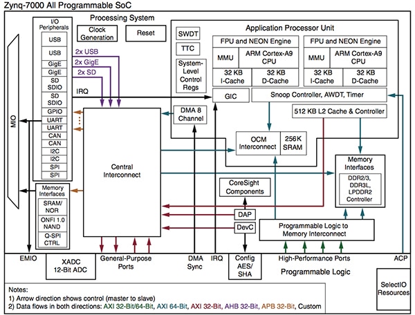
Figure 1: Xilinx Zynq SoC FPGA Block Diagram. (Courtesy of Xilinx)
In fact, the code developer can think of the programmable logic within the SoC as a hardware resource to be used to speed up sections of the code that would be too slow when implemented on the processor. One design team member might focus their activity on creating the hardware acceleration requested by the programmer or perhaps the programmer is able to implement the hardware themselves. Either way the algorithm becomes the focus for development with multiple implementation options available.
The SoC approach seems to work best when there are multiple performance- oriented algorithms going on simultaneously. One application area that has seen significant success with SoC FPGAs has been for complex image processing. These algorithms can usually be pipelined and/or parallelized, making them good candidates for FPGA acceleration. If the processor also needs to handle high bandwidth traffic on- and off-chip (perhaps with a high-speed serial interface and large off-chip buffer memories), additional hardware support to offload the low-level tasks from the processor may also pay a big dividend.
The multi-core response to SoC FPGAs
There are other approaches to implementing parallel and pipelined implementation for applications such as image processing. One approach taken by MCU vendors has been to implement multiple processing engines (multi-cores) on-chip to allow the designer to break up complex algorithms. When the architecture of each processor is the same it can be easy to take a complex algorithm and break it into pieces that each execute on a different, but functionally equivalent processor.
As an example, Texas Instruments offers the TMS320C66x multi-core fixed and floating-point Digital Signal Processor (DSP) that has eight DSP processors as well as a network coprocessor and a multi-core navigator to simplify data transfers using hardware queues (Figure 2). The DSP cores provide very high processing power for a wide range of complex algorithms such as audio, video, analytics, industrial automation, and media processing.
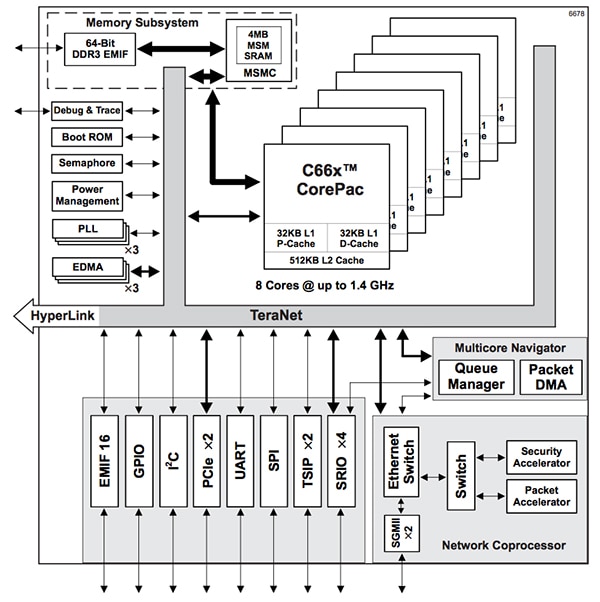
Figure 2: Texas Instruments Multi-Core DSP Block Diagram. (Courtesy of Texas Instruments)
Code development for a multi-core architecture is somewhat similar to that when using an SoC FPGA except the hardware acceleration is done by DSP cores instead of programmable fabric. When one core cannot implement the algorithm fast enough, just put another core to work on it. Keep doing this until you have run out of cores or have achieved your performance goals. Tuning and optimization can be required to get the last bit of power/performance efficiency, but some of the more advanced tools can help by providing performance and power profiles that help the optimization process.
Dual-core MCUs
The multiple core approach need not be used only for the highest performance applications. Often, SoC FPGAs can be found in less performance-bound applications where power and processing power need to be optimized. Because programmable fabric can be used to implement portions of the algorithm, the overall power required for implementation may be significantly less than a high-end DSP or multi-core solution.
MCUs manufacturers have also spotted this trend and have responded by putting dual-core processors to work on a single device. In some cases both a high-performance processor and a lower-performance processor are used. This allows a high-performance processor to implement the more complex part of the algorithm and the lower-performance processor to take care of the less complex management tasks. The lower-performance processor can be active a majority of the time, using less power than a high-performance core. (Note that multi-core systems can use a similar approach by only using as many cores as are required to hit the target performance level, dynamically. This is a bit more complex to implement, but can end up being very efficient if the algorithm requires a variety of performance levels that vary significantly over short periods of time.)
One example of a dual-core MCU that takes advantage of both a high-performance and a low-performance processor is the NXP Semiconductors LPC4350. Shown in Figure 3, below it has an ARM Cortex-M4 and a Cortex-M0. The M4 is used for the high-performance tasks while the M0 can be used for common management functions. In fact, the M4 sub-section can even be powered down if it is not needed and powered up when required by a processing request. This approach works well for algorithms that are only required periodically but need to process data with a quick response. Image processing on security cameras, as one example, can be very heavy when the image changes, but is not needed when the image is static.
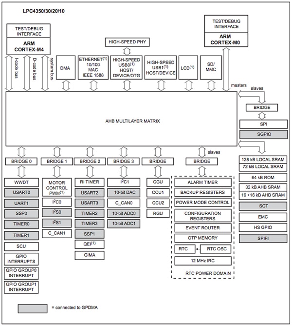
Figure 3: NXP Dual-Core MCU Block Diagram. (Courtesy of NXP)
Even the low end is programmable
Don’t think that only high- and medium-end MCUs are adding new twists to increase flexibility. Even low-end MCUs are adding programmable capabilities, perhaps not as a response to SoC FPGAs but as a way to pull small amounts of external logic “on-chip” the way programmable logic devices have been doing for decades. The Microchip PIC10F320 has added programmable logic, located in the configurable logic cell (CLC) block. A block diagram of the PIC10F320 with a more detailed view of the CLC is shown in Figure 4. The CLC can implement a wide variety of simple logic functions based on device inputs, internal clocks, internal peripherals, and register bits. The CLC even operates in low-power modes making it a convenient source for wake-up events to save a maximum amount of power when the MCU isn’t needed for processing.
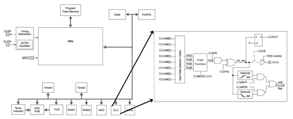
Figure 4: Microchip MCU with Programmable Logic Block Diagram. (Courtesy of Microchip)
The CLC is particularly useful on the PIC10F320 since it has only a few pins. Making the most of these pins and eliminating some external logic can make a big difference in board space requirements. One of the big advantages programmable logic offered even in the early days of PALs and CPLDs. Now with low-end MCUs putting programmable logic on chip, maybe we will see fewer low-end PLDs next to MCUs. Wouldn’t that be a new twist!
In conclusion, MCUs and SoC FPGAs solve similar applications problems and are beginning to compete for application dominance. Currently the challenge is primarily at the very high end of the application space, but recent innovations may broaden the applications overlap between MCUs and programmable devices.
For more information about the parts discussed in this article, use the links provided to access product pages on the DigiKey website.
免责声明:各个作者和/或论坛参与者在本网站发表的观点、看法和意见不代表 DigiKey 的观点、看法和意见,也不代表 DigiKey 官方政策。


