Low-Noise Switchers for Data Acquisition
投稿人:DigiKey 欧洲编辑
2013-01-22
Data-acquisition applications call for low-noise power supplies to be able to guarantee high performance and linearity. Traditionally, designers have used a combination of power-supply filtering and linear regulators to provide a stable supply. However, in recent years, manufacturers have developed low-noise switching regulator, for buck or boost operation, as well as for isolated power supplies that, in concert with relatively small ceramic capacitors, offer the low output ripple needed for data acquisition applications. This article provides an overview of low-noise, board-level, switched-mode power-supply options for data-acquisition systems. The devices discussed include Analog Devices’ ADP2114, Linear Technology’s LT3495, Microchip Technology’s MCP16301, and Texas Instruments’ TPS55010.
Designers of data-acquisition systems increasingly have to deal with two apparently conflicting requirements. One is to continue to improve the signal-to-noise ratio performance of their circuitry to satisfy the need for greater accuracy and repeatability in the target applications, which may range from strain-gauge interfaces for high-value manufacturing to mobile ultrasound scanners. The other is to reduce power consumption to improve battery life or to reduce the need for cooling fans. These two requirements have traditionally come into conflict in the design of the power supply.
Traditionally, the best option for designers of data-acquisition systems has been to use low-dropout (LDO) regulators between the main power supply and a circuit that uses an analog-to-digital (ADC) converter. The use of a linear power source helps to filter out unwanted noise from the main power supply, which normally uses a switched-mode topology for its efficiency benefits.
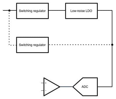
Figure 1: Traditional data-acquisition power architecture versus the alternative approach using a low-noise switched-mode regulator.
One problem is that switching topologies used in, for example, buck regulators, can result in the switching of large voltages at high frequencies. This results in ringing and ripple on the supply rail that acts as a source of noise for the ADC. The issue can be exacerbated by the use of CMOS technology, which is now in common use even in high-speed, high-accuracy devices because of its excellent power-consumption characteristics. The power-supply rejection ratio of CMOS can be lower than that of ADCs fabricated using bipolar or BiCMOS technology.
As a result, there are very good reasons for using linear-topology supplies such as LDO regulators as the direct energy source for an ADC, even though they will generally increase power consumption overall.
Although LDO regulators are designed to minimize the voltage drop on the supply rails, there is still the requirement for a small dropout voltage for the regulators to function well. This dropout voltage is usually in the order of 200 mV to 500 mV, although for convenience of design it may be more than 1 V. For example, the main switched-mode power supply may provide a 5 V output for use by other modules within the circuit, and that is then dropped to 3.3 V or lower for use by many of the key components. The energy lost through the dropout voltage can be calculated as a percentage of the dropout versus the required LDO output. This lost energy is generally dissipated as heat, which can increase product size through the use of heatsinks and fans.
The efficiency of a switching regulator is not generally related to the difference between input and output supply rails but to the way in which the regulator delivers charge packets to a filtered output. Through the use of resonant switching and other techniques, such regulators can minimize the losses from switching events. High frequency switching reduces the size of passive components and their related losses. The issue is how well the output of the regulator can be filtered to reduce the output supply-rail ripple that results in increased noise within ADC circuits.
One option is for the designer to employ filtering on a standard DC/DC converter. Generally, this filter comprises a ferrite bead and a set of bypass capacitors. However, there are a number of considerations that need to be taken into account during ferrite-bead selection. The bead needs to have a low direct-current resistance (DCR) to minimize the voltage drop across the bead. It should also be current rated to be sufficient for the data converter, although this should be the case for many beads with the growing number of low-power data converters on the market.
The ferrite bead should be selected so that its impedance is sufficiently high at the switching frequency of the DC/DC converter, and preferably at its major harmonic frequencies as well, to ensure effective blocking of the regulator’s switching noise. Some manufacturers of DC/DC converters recommend the use of shielded ferrite core inductors because of their low core losses.
It is possible to achieve better noise performance with DC/DC converters and regulators that have been designed with the needs of data-acquisition circuitry in mind. Manufacturers have responded to the need for higher-efficiency low-noise power supplies with switching regulator designs that use a combination of filtering and improved control algorithms to reduce interference. One example is the Analog Devices ADP2114.
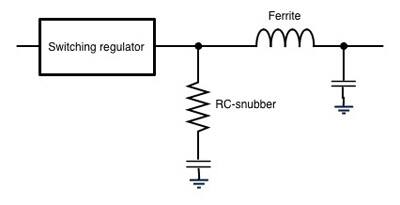
Figure 2: The combination of RC snubber to control slew and ferrite bead with bypass capacitor can reduce noise on the output supply rails.
The ADP2114 is a dual-channel buck regulator which has its two channels, which are under pulse-width modulation (PWM) control and phase shifted by 180°C. If they are used together, the phase shift can be employed to reduce ripple current as well as for a reduction in the size of input capacitors.
In addition to the use of phase shifting, the ADP2114 has its gate slew rate tuned to minimize electromagnetic interference, suiting the device to use in sensitive data-acquisition circuits. The slew rate within a regulator can be controlled by adjusting the size of the driver devices. Fast slewing will generally reduce transmission losses, but the consequences of parasitic inductances can lead to the serious EMI issues encountered with conventional switched-mode DC/DC converters.
The internal switching frequency of the ADP2114 can be set to 300 kHz, 600 kHz, or 1.2 MHz to allow optimization of the input/output voltage ratio and to control the size of the external passives. The operating frequency can also be synchronized to an external clock up to 2 MHz. A bidirectional synchronization pin can be used to provide a 90° shifted output clock that runs at double the internal frequency so that multiple devices can be used together to increase the overall power output – and avoid the beat frequencies and unwanted EMI that result from unsynchronized converters. Alternatively, the strategy can be used to reduce ripple in an interleaved configuration even further.
The use of pulse-skip mode lets the designer choose between ripple performance and energy efficiency when dealing with light load conditions – which may be situations when the ADC is inactive, thereby reducing the requirement for low ripple. Under light-load conditions, the size of each charge packet delivered to the output capacitor is at or close to minimum levels. This results in comparatively high switching losses compared to the amount of energy converted for use by the load. Through pulse skipping, these switching losses can be reduced by placing greater reliance on the energy stored in output capacitors.
In pulse-skip mode, the DC/DC converter only switches into PWM mode when the output voltage drops below a programmed threshold. This replenishes charge in the output capacitor and boosts the output voltage temporarily. The DC/DC converter then saves power by not switching until the voltage passes the threshold again and the next charge pulse is delivered. A consequence of this is that the overall ripple increases, albeit with a lower frequency than that encountered in full PWM mode. If the magnitude of this ripple is too high then the designer can force PWM mode at all times by controlling the status of one of the regulator’s control pins.
Analog Devices designed the ADP2114 to allow for low ripple with small inductors. But the designer has a degree of latitude in the size of the inductors that can be used – the trade-off is one of power losses and ripple performance versus transient response. A small inductor leads to larger inductor current ripple and lower efficiency but better transient response. The output capacitor can also be relatively small because of the high switching frequency. As a result, ceramic capacitors can be used, although it is better to use those with X5R or X7R dielectrics rather than Y5V or Z5U, as they have poorer temperature characteristics. The higher the capacitance, the lower the output voltage ripple, and capacitances tend to range from 10 µF to 100 µF.
The MCP16301 from Microchip Technology is a buck regulator with integrated switch that can be used with noise-sensitive circuitry and which will operate with input voltages up to 30 V. This suits the regulator to environments, such as industrial control, where 24 V DC sources are commonly used.
Like the ADP2114, the MCP16301 uses high frequency switching to minimize the size of external filter components and to help reduce the PCB real estate needed for the power supply. The device supplies up to 600 mA of current at voltages from 2 V to 16 V. To control switching noise, the MCP16301 can be used with an RC snubber or a resistor to limit the switching speed of the internal N-channel MOSFET.
In some cases, a boost converter is needed to provide low-noise power to ADCs and analog circuitry that need to operate with power supply rails set to a voltage that is achievable under battery power, or where the primary system rails operate at 3 V or 5 V. An example of this type of DC/DC converter is the LT3495 from Linear Technology, which uses a combination of control over peak inductor current and switch-off time to reduce output ripple. However, the switch’s off time is not allowed to exceed a certain threshold to ensure that the frequency of operation does not descend into audio band, causing distracting noise to users even at light loads.
The LT3495 is designed to work with inductors with a value of 3.3 µH or more to ensure high performance, preferably with low core losses. For full output power, the inductor should have a saturation current rating that is higher than the peak inductor current. As with other DC/DC converters, the capacitors used for output filtering can be ceramics, but should be of the X5R or X7R variety to ensure good temperature compatibility and that the effective capacitance is not badly affected by applied voltage. A capacitor of between 1 µF and 10 µF generally provides a good trade-off between ripple and transient response. The LT3495 has an input voltage range of 2.5 V to 16 V, and can generate voltages of up to 40 V.
Isolation is an important part of many data-acquisition systems, especially those that go into the industrial environment where noise may be transmitted by serial channels and other connectivity options. For this purpose, Texas Instruments developed the TPS55010 to act as a transformer driver that can provide isolated power for RS485 and RS232 interfaces. The device uses fixed-frequency current-mode control and feedback to regulate the output voltage for power outputs of up to 2 W. Switching frequency can vary from 100 kHz to 2 MHz to allow a trade-off between board space, efficiency and noise.
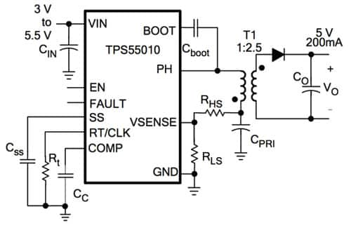
Figure 3: Block diagram of the TPS55010 regulator for isolated power supplies.
Through devices such as the low-noise switching regulators mentioned above and the use of filtering techniques, it is now feasible to design out LDOs from sensitive data-acquisition circuitry.

免责声明:各个作者和/或论坛参与者在本网站发表的观点、看法和意见不代表 DigiKey 的观点、看法和意见,也不代表 DigiKey 官方政策。




 中国
中国